Samsung Electronics has begun moving a key component in its next generation of advanced memory: non-destructive inspection of hybrid bonding. According to the Korean media TheElec, the company is already validating new equipment capable of detecting micro-defects at the bonding interfaces, with Onto Innovation among the leading providers in this initial phase. Although Samsung has not yet formalized this move with a detailed announcement regarding tools, volumes, or timelines, it aligns with a trend the company has publicly hinted at: the shift of HBM toward denser, hotter architectures that are much more challenging to manufacture.
The crucial factor lies in the type of defect they aim to prevent. In hybrid bonding processes, small voids, misalignments, or interface defects can spoil highly valuable wafers or increasingly costly memory stacks. Conventional optical inspection begins to show limitations, especially when layered metallic structures, stacked architectures, and opaque materials are involved. Therefore, interest is shifting toward nondestructive technologies based on laser ultrasound and X-ray methods, capable of “seeing” beyond the surface without damaging the product during quality control.
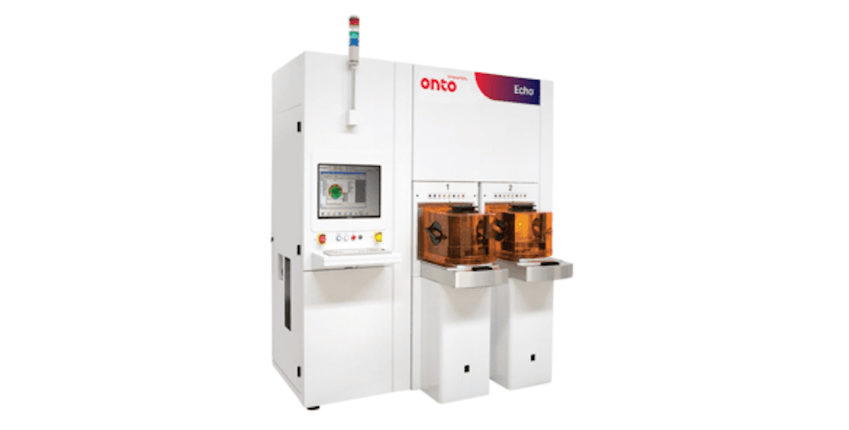
Onto Innovation Gains Advantage in an Open Race
According to TheElec, Onto Innovation reportedly has a joint development program with Samsung and has supplied equipment to production lines for validation. This information, sourced from industry insiders cited by the Korean media, should be read as supply chain intel rather than a confirmed public statement from Samsung. Nonetheless, the external context supports that Onto is gaining influence in this area. The company announced on March 16 the launch of its Dragonfly G5 system and stated that a major HBM manufacturer had completed evaluation and selected it for 2D inspection during the HBM4 ramp, with shipments expected from Q2 2026. While that client was not publicly identified, the timing aligns closely with movements attributed to Samsung.
Onto’s interest extends beyond traditional visual inspection. The company has been working with ultrafast acoustic techniques applied to advanced packaging for some time. In technical documentation published in 2025, it described alongside Samsung Electronics how its picosecond-scale ultrasonic technology can measure metallic layer thicknesses and interconnect structures in high-performance AI packages. The principle is sophisticated but straightforward: a laser pulse generates an acoustic wave that propagates through the structure, bounces at internal interfaces, and is detected by another laser sensor to reconstruct information that optical inspection cannot accurately resolve.
This capability is especially valuable in hybrid bonding, where the quality of the joint between layers influences not only electrical performance but also thermal dissipation, reliability, and overall process performance. Onto also notes that its PULSE metrology is a contactless, nondestructive technique designed for inline multilayer measurements on product wafers—becoming increasingly relevant as backend processes mirror frontend precision and complexity.
The 16-Layer HBM Demands a New Inspection Approach
This news is more than just a purchase announcement; it arrives at a critical moment. Samsung showcased its HCB (hybrid copper bonding) technology at NVIDIA GTC 2026, claiming this method will enable the next generation of HBM to reach 16 layers or more, while reducing thermal resistance by over 20% compared to thermal compression bonding (TCB). It also unveiled HBM4E with 16 Gbps per pin and 4.0 TB/s bandwidth for the first time, positioning its HBM4 already into mass production for NVIDIA’s Vera Rubin platform. This reflects a concrete roadmap for ultra-dense memories, not just a distant concept.
When a company plans to stack more layers, lower thermal resistance, and boost pin performance, interface inspection shifts from a factory detail to a key competitive factor. The denser the stacking, the more costly it becomes to detect bonding defects late in the process. For wafers or HBM stacks of higher value, the pressure to identify faults without destroying the product during testing increases. From this perspective, investing in new inspection tools is not optional but essential for achieving acceptable yields in HBM4E and future generations.
An industry perspective suggests that Samsung isn’t just engaging with Onto; it is also interacting with other vendors equipped with ultrasonic and X-ray technologies, including several Korean groups that could lead to joint adoption programs starting in Q2. If confirmed, Samsung would be developing not only a more sophisticated inspection flow but also broadening its supplier base. As AI continues to strain the entire semiconductor value chain, relying on a single technique or provider is no longer a practical strategy for anyone.
Enhanced Process Control for an Increasingly Demanding Memory Market
This strategic move goes well beyond laboratory testing. Competition in HBM today is driven by performance, power consumption, thermal management, stacking capacity, and delivery times. Samsung must improve its standing against formidable rivals in advanced memory, which requires refining both design and manufacturing processes. Nondestructive inspection of hybrid bonding aligns precisely with these goals: minimizing losses, elevating quality control, and paving the way for memories with more layers, higher bandwidth, and fewer errors.
More broadly, Samsung signals where the next bottlenecks might be. While the market often focuses on GPUs, interposers, or process nodes, there is increasing value in technologies that allow verification, alignment, and validation of extreme stacking without damaging the component. If hybrid bonding is to be central to the new-generation HBM, inspecting that bonding process will also become a strategic priority.
Frequently Asked Questions
What is hybrid bonding in HBM memories?
An advanced bonding technique that directly fuses copper surfaces between chips or wafers, eliminating the need for microbumps used in other methods. Compared to thermal compression bonding, it reduces thermal resistance and improves electrical characteristics, which is essential in multilayered stacked memories.
Why does Samsung need new inspection equipment for hybrid bonding?
Because internal defects such as voids or misalignments are difficult to detect with conventional optics and can ruin costly wafers or HBM stacks. New nondestructive techniques enable inspection of opaque layers and buried structures without damaging the product.
What role does Onto Innovation play in this development?
Onto is positioned as a leading supplier in the supply chain reports. It has announced that a major HBM manufacturer has chosen its Dragonfly G5 system for HBM4 ramp inspection and has previously collaborated with Samsung on ultrasonic metrology for advanced packaging.
Does this indicate that Samsung will use hybrid bonding in HBM4E or HBM5?
Samsung publicly demonstrated its HCB (hybrid copper bonding) technology at GTC 2026 for 16+ layer HBM, linked to thermal improvements over TCB. While not confirming specific product plans, this strongly suggests that hybrid bonding will be part of their next-generation HBM roadmap.
via: thelec.kr