Russia has officially announced the production of its first national lithographic scanner, capable of manufacturing chips at 350 nanometers (nm). This advancement, while it may seem modest compared to current leading-edge nodes, represents a significant milestone in the country’s quest for technological independence in a key sector like semiconductors.
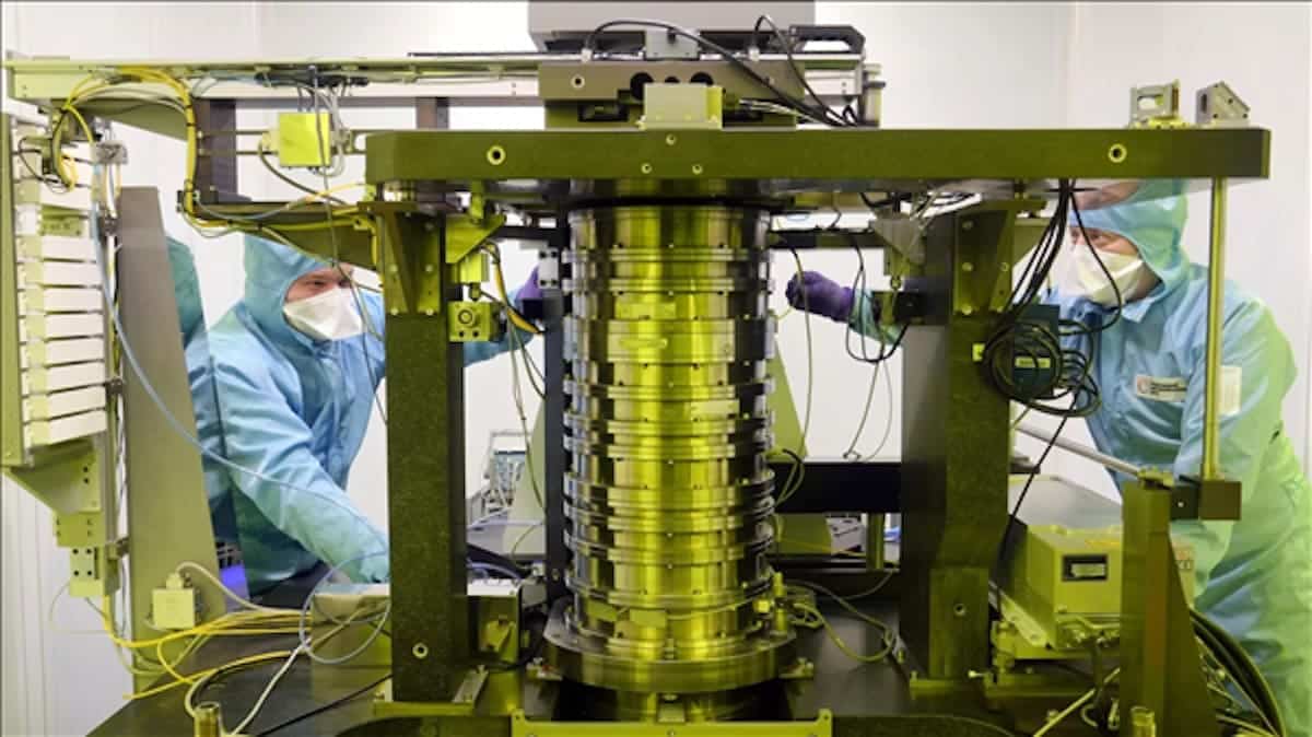
The announcement was made by Moscow’s mayor, Sergei Sobyanin, who emphasized not only the industrial importance of the achievement but also its geopolitical dimension. “There are fewer than ten countries in the world capable of producing this type of key semiconductor equipment, and Russia has become one of them,” he stressed while sharing the first image of the device.
A Robust and Functional Design
The 350 nm lithographic scanner has been completely designed and assembled in Russian territory. Unlike many foreign machines that still use mercury lamps as a light source, this model opts for solid-state lasers, which promise greater efficiency, spectral accuracy, durability, and reduced environmental impact.
The machine can work with wafers of up to 200 mm in diameter and cover an exposure area of 22 x 22 mm, a format that meets the requirements of various industrial applications, especially in sectors where advanced processes (such as 7 nm or below) are not strictly necessary, such as automotive, energy, or telecommunications.
Beyond 350 nm: Ambitious Plans for 2026
This development is not an isolated project. According to the timeline revealed by Russian authorities in 2023, by 2026, a national machine capable of operating at the 130 nm node is expected to be ready, with an eye on 65 nm, a technology that Russia already masters but still depends on imported scanners.
With active development facilities in Moscow, Zelenograd, St. Petersburg, and Novosibirsk, the country aims to move towards a complete “nationalization” of its chip manufacturing processes. The timely adherence to the schedule in the development of the 350 nm machine is a sign that the plan is serious, something rarely seen in such technologically complex projects.
Collaboration with China?
One aspect that has sparked interest is the potential collaboration with China, a country that is also developing its own lithographic technology using solid-state laser sources for DUV (deep ultraviolet) lithography, even aiming to reach 3 nm. Although there is no official confirmation, the technological similarities suggest a possible shared design or strategic cooperation between the two countries, which share the ambition to reduce their dependence on Western technologies.
A Race for Technological Self-Sufficiency
Lithography is one of the most complex pillars of the semiconductor manufacturing chain and has historically been dominated by players like ASML in Europe or Canon and Nikon in Asia. In this context, Russia’s move—though lagging in terms of miniaturization—reinforces its position in the global race for technological sovereignty in an increasingly polarized geopolitical world.
For now, 350 nm may seem like a slow train compared to the 3 nm or 5 nm nodes that lead the industry, but for Russia, it is the right car toward its industrial independence. And the next destination, 130 nm, is already on the horizon.
via: Mydrivers