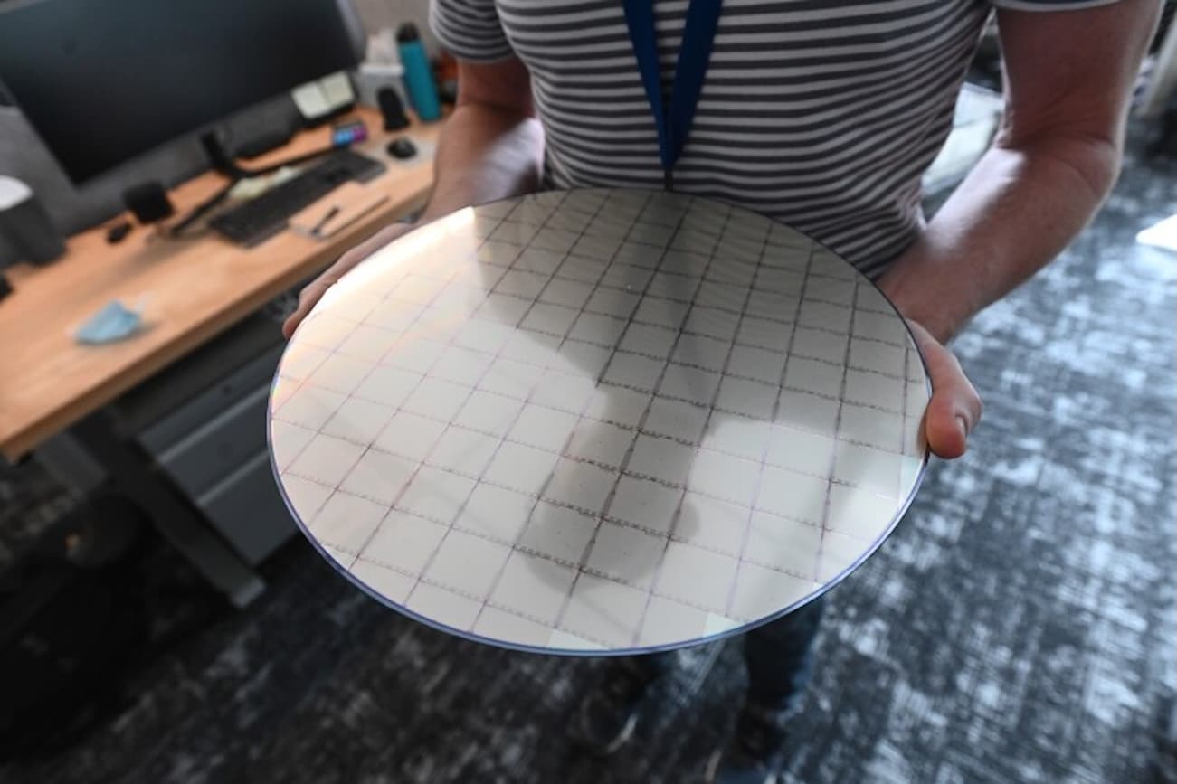
The Japanese company Rapidus has reached a new milestone in its ambitious plan to compete with giants like TSMC, Samsung, and Intel: it has officially begun pilot production of wafers with gate-all-around (GAA) transistors at 2 nanometers at its IIM-1 facility in Japan. According to the company, the initial wafers already demonstrate the expected electrical characteristics, indicating that the technological development of its process is progressing as planned.
This step marks the beginning of a critical phase: verifying that transistors produced with this advanced technology meet key parameters such as threshold voltage, leakage current, switching speed, and energy consumption. Although Rapidus has not disclosed exact figures, the fact that wafers are already “flying” in production shows that their manufacturing environment is functional.
### A different strategy: processing wafers one by one
Beyond technological advances, what truly sets Rapidus apart is its full commitment to single-wafer processing. Unlike other manufacturers—who combine batch processing and individual processing depending on the stage—Rapidus has chosen to apply the single-wafer approach in all steps of the process, including traditionally grouped ones like oxidation, ion implantation, cleaning, or annealing.
Although this method is more costly and yields less per tool compared to batch processing, it allows engineers to adjust each parameter in real-time and customize the treatment of each wafer according to its characteristics. The benefit: earlier detection of anomalies, faster correction of errors, and the generation of large volumes of high-resolution data per wafer.
These data, fed into AI algorithms, will enable Rapidus to implement continuous process improvements (CPI) and more effective statistical process control (SPC). In the medium term, this approach could lead to lower defect rates, higher yields, and reduced variability among chips.
“This processing architecture is ideal for quickly adapting to new designs and small production runs, which is essential for niche clients and specialized applications in artificial intelligence,” say sources close to the company.
### Infrastructure, tools, and market outlook
Construction of the IIM-1 plant, which began in September 2023, has advanced rapidly. By the end of 2024, it was equipped with cutting-edge DUV and EUV lithography tools. Successful EUV lithography exposures were performed in April 2025, and since then, the factory has connected more than 200 specialized pieces of equipment.
With these developments, Rapidus aims to position itself as a key player in the new generation of GAA chips, whose demand is expected to grow exponentially with the rise of AI, HPC, and edge computing applications.
To facilitate early adoption of its technology, the Japanese firm announced that its first process design kit (PDK) will be available in the first quarter of 2026, allowing designers and clients to prototype chips using Rapidus technology either at their own facilities or at the IIM-1 plant.
### Challenges and long-term vision
Rapidus’ innovative approach is not without challenges. Single-wafer processing involves greater operational complexity and higher per-chip costs in the initial stages. However, in a context where each defect or variation in 2nm chips could mean millions in losses or failures in critical systems, precision is everything.
“Rapidus’s gamble is clear: sacrifice speed for control, volume for reliability. In a world where AI is redefining everything, that might be the only winning move,” says an industry analyst.
With this strategy, Japan reasserts itself as a key player in the global semiconductor industry, blending innovation, precision, and technological sovereignty in one of the most advanced technologies in history.
via: tomshardware