
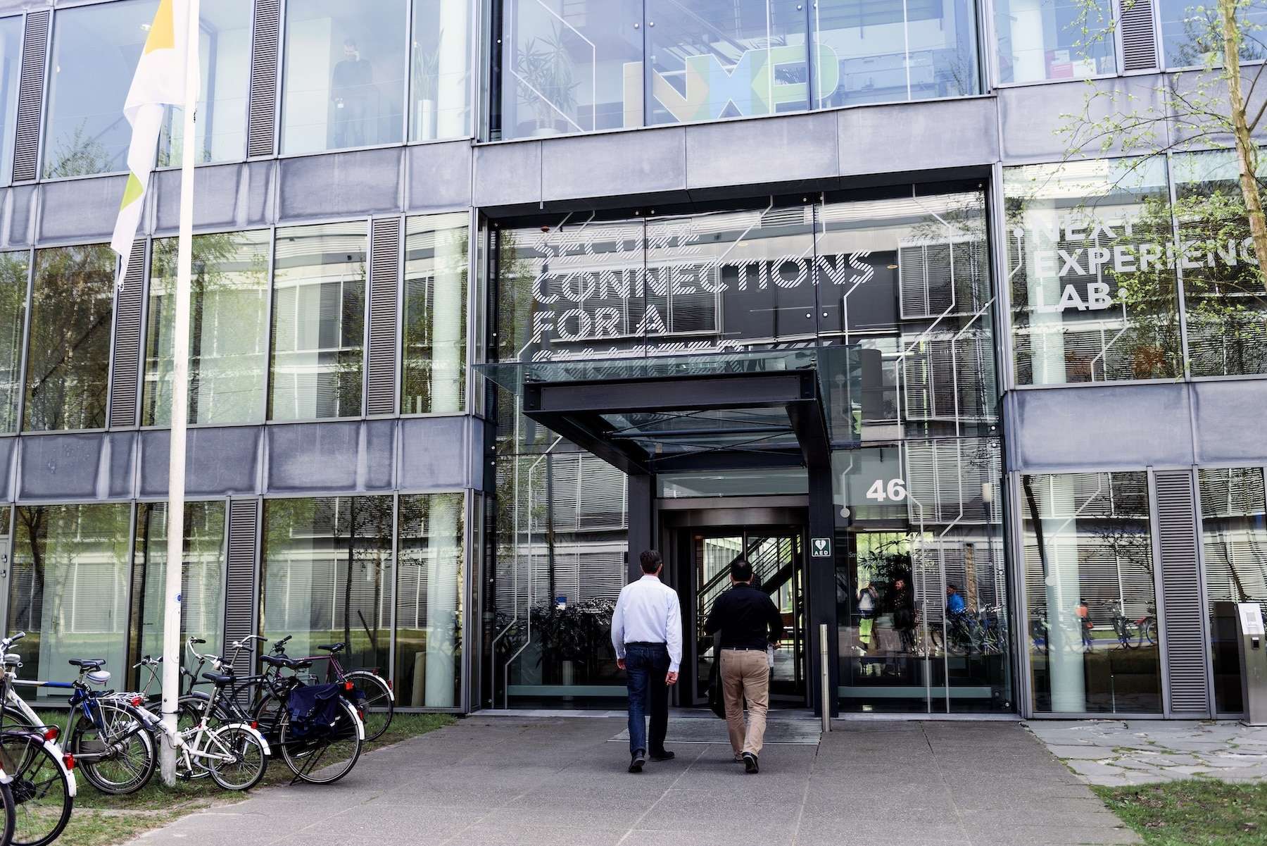
NXP Semiconductors will significantly expand its chip assembly and testing capacity in Petaling Jaya, Malaysia, with a new factory that will add approximately 46,500 square meters of production space. The facility is expected to begin increasing production in the first quarter of 2028 and, once fully operational, will more than double the current capacity of the complex. This decision also has a broader strategic meaning: NXP is preparing now for the backend capacity it will need to process future chips from new wafer fabrication plants in Singapore and Dresden.
The key points of NXP’s expansion in Malaysia in 30 seconds
- NXP will add about 46,500 m² of production to its Petaling Jaya site, reaching approximately 83,600 m².
- The new assembly and testing capacity will start growing during the first quarter of 2028.
- Total site production should more than double when the expansion reaches its planned full capacity.
- The plant will handle production associated with VSMC in Singapore and ESMC in Dresden.
- NXP is investing in automation, traceability, and greater internal control over the final manufacturing stages.
This expansion serves as a reminder of something often overlooked in the semiconductor conversation. Building new wafer fabs is of limited use if there isn’t sufficient capacity to dicing, encapsulation, electrical bonding, inspection, and testing before chips are shipped to automakers, industrial equipment manufacturers, or electronic device makers.
This work is part of what’s known as the backend manufacturing process.
And NXP is aiming to prevent that stage from becoming the next bottleneck.
46,500 more square meters and a highly automated factory
The new facility will expand NXP’s current Petaling Jaya center by around 500,000 square feet, approximately 46,500 square meters.
Once completed, the entire complex will boast roughly 900,000 square feet of manufacturing space, close to 83,600 m². NXP expects to begin phased production increases in the first quarter of 2028, with total capacity more than doubling by full operation.
The company has not disclosed investment costs or specific yearly chip processing volumes yet, so its final capacity can’t be directly compared to other major assembly sites.
However, it has shared some details about the technology to be used.
The facility will be designed as a highly automated smart factory, equipped with automatic material handling systems, known as AMHS (Automated Material Handling Systems), and advanced quality management technologies.
In a semiconductor factory, this automation goes far beyond replacing human labor with robots carrying boxes.
Each batch can follow different paths depending on the product, encapsulation, testing requirements, available machinery, and customer specifications. An automated system can maintain the identity and traceability of materials as they move through various stages.
Quality management is equally critical for NXP because a significant portion of its products are used in automotive and industrial sectors, where a field failure could have much more serious consequences than a consumer electronic component failing.
Data collected during manufacturing and testing can be linked to the original batch, equipment used, materials, and process conditions to identify anomalies before they impact large volumes.
Malaysia will process some chips arriving from Singapore and Germany
The 2028 timeline also appears strategic, not coincidental.
NXP is simultaneously involved in two major 300mm wafer projects: VSMC in Singapore and ESMC in Dresden.
The company notes that the additional capacity in Petaling Jaya will support the expected production needs of both facilities.
VSMC, or VisionPower Semiconductor Manufacturing Company, is a joint venture created by Vanguard International Semiconductor (VIS) and NXP. VIS holds a 60% stake, NXP owns 40%.
The project involves a 300 mm wafer fab in Singapore with an initial investment estimated at $7.8 billion. Its first production is targeted for 2027, aiming to reach about 55,000 wafers per month by 2029.
The plant will process designs in roughly 130 to 40 nanometers for applications including analog, power management, mixed signal, and other sectors serving automotive, industrial, consumer, and mobile markets.
While these are not the cutting-edge 2 or 3 nanometer nodes making headlines, they are suitable for many applications where reliability, cost, voltage handling, lifespan, and availability are more important than transistor size.
The other major project is in Europe.
ESMC, European Semiconductor Manufacturing Company, is a joint venture in Dresden including TSMC, Bosch, Infineon, and NXP. TSMC controls 70%, while Bosch, Infineon, and NXP each hold 10%.
This fab plans for an estimated investment exceeding €10 billion and aims to produce around 40,000 300 mm wafers per month, utilizing 28/22 nm and 16/12 nm processes TSMC will provide. Initial production was expected at the end of 2027, but NXP’s latest annual report now projects start in 2028.
This schedule shift underscores why future fab timelines should be viewed as goals rather than guaranteed dates.
A wafer fab doesn’t complete the chip
The connections between Singapore, Dresden, and Malaysia highlight how this complex supply chain really works.
VSMC and ESMC will produce wafers.
But once processed, a wafer still contains hundreds or thousands of integrated circuits that are not yet the final components purchased by customers.
Another manufacturing chain begins after wafer fabrication.
Individual chips must be separated, encapsulated, electrically bonded, tested, inspected, and prepared for shipment.
A significant increase in frontend capacity naturally creates a corresponding need for backend processing.
Thus, building a large wafer fab without simultaneously planning backend operations can limit overall production availability for customers.
NXP appears to coordinate both processes: adding wafer capacity in Europe and Singapore while ramping up assembly and testing in Malaysia before those fabs are fully operational.
Its annual report also confirms that NXP keeps a substantial portion of its assembly and testing activities in-house, combining internal manufacturing with external partners.
NXP’s hybrid manufacturing strategy
The company describes this approach as a hybrid manufacturing strategy.
It does not aim to manufacture every transistor for every product internally.
Instead, it combines own fabs, joint ventures, and contracted capacity depending on technology and product needs.
For example, in VSMC, NXP will have rights to 40% of the capacity, and in ESMC, 10%.
This model allows securing a portion of production without bearing the full costs of building and operating new wafer fabs alone.
The Malasia expansion also increases direct control over final assembly and testing stages.
However, this doesn’t make NXP’s supply chain entirely self-sufficient.
Chip assembly requires substrates, leadframes, encapsulant materials, chemicals, testing equipment, handlers, and numerous components sourced from international suppliers.
NXP’s own annual report acknowledges dependence on a limited number of suppliers for some materials, noting that the industry has increasingly relied on long-term supply agreements to secure capacity after past shortages.
Resilience stems from having more alternatives and avoiding reliance on a single supplier or location for critical process steps.
Malaysia’s decades-long role in NXP’s supply chain
NXP’s presence in Malaysia is not new—it’s been operating there since 1972. Over five decades, the country has developed skilled workers, suppliers, logistics, and semiconductor expertise.
This environment is difficult to rapidly replicate elsewhere.
While the US, Europe, and Japan are investing heavily in new wafer fab plants, much of global assembly and testing remains concentrated in Asia.
Malaysia specializes precisely in these stages and is now seeking to move toward higher automation and value-added activities.
NXP also collaborates with Malaysian universities for engineer training and R&D—a strategic move as countries compete for semiconductor talent.
Automation doesn’t eliminate the need for human expertise.
Factories with automated material handling require process engineers, maintenance specialists, industrial software experts, sensors, networking, data analysts, and cybersecurity professionals.
The more connected the production, the greater the dependence on reliable digital infrastructure.
The next bottleneck may not be in wafer fabrication
The Petaling Jaya expansion reflects a significant shift within the industry.
The global chip shortage earlier this decade demonstrated that capacity must be viewed as a full supply chain—silicon availability, encapsulation, substrates, equipment, and qualified processes all matter.
A fab might be ready, but if encapsulation equipment or substrates are short, production stalls.
Similarly, a factory might be finished but lack the necessary equipment or qualified processes to meet volume targets.
NXP is working to synchronize these stages.
VSMC in Singapore is scheduled to start production in 2027, ESMC targets 2028, and Petaling Jaya will also ramp capacity beginning in early 2028.
In theory, the schedules align.
The real challenge comes after: installing equipment, qualifying processes, stabilizing yields, and transforming hundreds of thousands of square meters of factory space into actual production.
In semiconductors, unveiling a new facility is just the beginning; the real work starts afterward.
Frequently Asked Questions
What is NXP building in Malaysia?
NXP is expanding its semiconductor assembly and testing facility in Petaling Jaya. It will add about 46,500 m² (approximately 500,000 square feet) of operational space.
When will the new NXP factory begin production?
The company expects to start phased capacity increases in the first quarter of 2028. Full capacity ramp-up will follow a period of commissioning and qualification.
How does the Malaysia plant relate to the new factories in Singapore and Dresden?
NXP states that the additional assembly and testing capacity will support the production growth expected from its ecosystem, including future capacities at VSMC in Singapore and ESMC in Dresden.
What’s the difference between wafer fabrication and chip assembly?
Wafer fabrication creates the circuits on silicon. Afterwards, the individual dies are separated, encapsulated, electrically bonded, tested, and inspected before becoming components ready for customer delivery.
via: industrialnews
