Sure! Here’s the translation to American English:
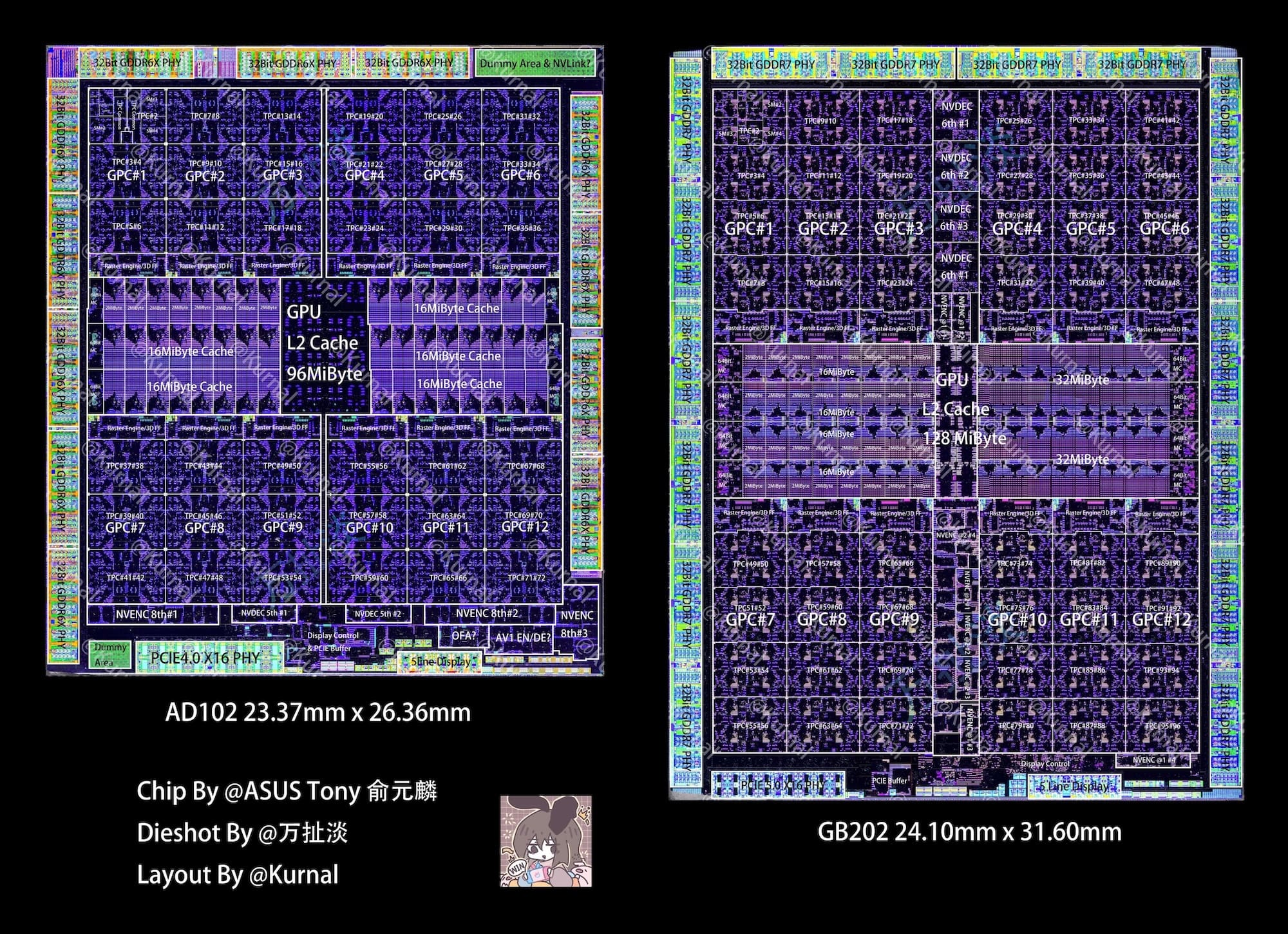
The Blackwell architecture by Nvidia, which powers its new flagship graphics card, the RTX 5090, has begun to reveal its true potential. A detailed diagram of the GB202 chip was recently shared on the social media platform X, showcasing the intricate arrangement of its components. This design is a prominent example of Nvidia’s ambition in its quest to dominate the high-performance GPU market.
The Heart of the GB202: Optimized Design and Enhanced Capacity
The GB202, the central chip of the RTX 5090, is 24% larger than its predecessor, the AD102, used in the Ada Lovelace-based RTX 4090 series. At 761.56 mm² compared to the AD102’s 616 mm², Nvidia has significantly increased the physical capacity of the chip, aiming for performance enhancements and expanded capabilities.
At the core of the GB202 is the L2 cache, organized in layers of 32 MB divided into blocks of 2 MB. This design optimizes data flow within the chip, facilitating resource-intensive tasks like graphics processing and memory management. Surrounding the L2 cache are 12 Graphics Processing Clusters (GPC), each with several Texture Processing Clusters (TPC). In total, the chip boasts 96 TPCs, which in turn house Streaming Multiprocessors (SM), critical components that include CUDA cores and L1 cache.
Additionally, the GB202 features 12 blocks of rasterization/3D FF engines. These units are responsible for converting geometric representations into visible images on the screen, an essential task for rendering high-quality graphics.
Key Features: From Memory to Video Controllers
The GB202 also stands out for its robust memory design. On either side of the L2 cache are eight 64-bit memory controllers, while the top, left, and right sides of the chip house 32-bit GDDR7 physical interfaces that connect the GPU to high-speed memory modules. This ensures optimal performance even in the most demanding tasks.
In the center of the chip, from top to bottom, Nvidia has integrated video encoders and decoders (NVDEC and NVENC). These units provide advanced capabilities for video playback and recording, solidifying the RTX 5090 as an ideal option for content creators and demanding users.
At the bottom of the GB202 lies the physical interface PCIe 5.0 x16 along with the display controller, ensuring seamless connectivity with other components and flawless graphical output.
Comparison with Ada Lovelace: The Impact of TSMC N4P
The production of the GB202 is carried out using TSMC’s N4P node, an enhanced version of the N4 process used in Ada Lovelace. This technological shift explains the increase in the physical size of the GB202 compared to its predecessor, even though it offers significant improvements in terms of efficiency and performance.
Despite its impressive size, the GB202 is not Nvidia’s largest chip. This title still belongs to the Hopper and Volta architectures, whose chips GH100 and GV100 reached 814 mm² and 815 mm², respectively.
A Milestone in Graphics Innovation
The GB202 represents a leap forward in GPU architecture, standing out not only for its size but also for its optimized design and massive processing capacity. With its Blackwell architecture, Nvidia continues to push the boundaries of what is possible in the realm of graphics cards, cementing its leadership in a highly competitive market.
For enthusiasts, developers, and high-performance professionals, the RTX 5090 with the GB202 chip promises to redefine the standards of graphical power and open new opportunities in content creation, gaming, and compute-intensive applications.
https://twitter.com/Kurnalsalts/status/1883153126011892140
via: Tom’s Hardware and X @Kurnalsalts