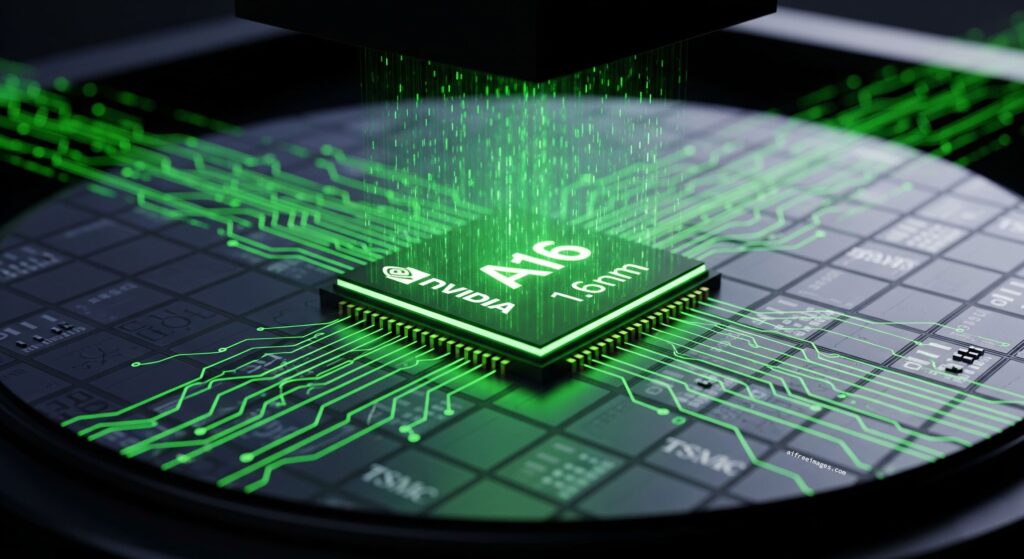
The semiconductor industry landscape is taking an unexpected turn: NVIDIA is emerging as the first customer for TSMC’s A16 node, a 1.6 nm process with backside power delivery and GAAFET (Gate-All-Around) transistors that will mark a technological leap forward in the second half of the decade.
Until now, NVIDIA had followed a different strategy compared to Apple or Qualcomm, which often debuted the most advanced nodes. Jensen Huang’s company preferred to maximize mature architectures and processes, reserving cutting-edge nodes for others. However, the seem to have changed the rules of the game.
From 110 nm to the quantum leap of A16
According to sources cited by Ctee (China Times), NVIDIA hadn’t led the adoption of leading-edge nodes since the 110 nm. Since then, it focused its competitiveness on architectural advancements. Now, with the arrival of A16, it plans a move that could align with its future architectures, Rubin Ultra or, more likely, Feynman, scheduled for 2027-2028.
The A16 is not just a scaling reduction. It represents:
- The introduction of GAAFET nanosheets, improving energy efficiency.
- The adoption of Super Power Rail (SPR) or backside power delivery, reducing electrical resistance and increasing density.
- A significant increase in performance per watt, critical for AI data centers.
A bet driven by AI and competition
The market is no longer dictated solely by smartphones. High-performance AI (HPC/AI) has become the growth lever for TSMC. According to reports, after the launch of AMD’s Venice CPUs in 2 nm, NVIDIA plans not to be left behind and aims to leap to the A16 node.
However, the cost is high:
- A chip in 2 nm from Apple costs around $27,000 per wafer.
- With A16 backside power, the cost could surpass $30,000 per wafer.
Nevertheless, density and efficiency justify the investment in a context where major clients are “paying for value,” not just volume.
Spain and Europe: a strategic context
This news arrives as Europe promotes its European Chips Act to reduce dependence on Asian and North American suppliers. While TSMC maintains its technological leadership from Taiwan, NVIDIA’s entry into the A16 node confirms that the battle for technological sovereignty is inevitably fought by those setting the pace of miniaturization.
A cycle shift for TSMC
For two decades, smartphones were the main drivers of the most advanced processes. Now, AI chips for data centers are taking over. This move not only diversifies TSMC’s customer base but also ensures that future milestones of Moore’s Law are linked to the rise of accelerated computing and artificial intelligence.
For NVIDIA, this is a strategic play: to stay ahead of the competition and secure capacity in a node that promises to be as transformative as the 28 nm or 7 nm nodes once were.
FAQ
What is the TSMC A16 node?
It is a 1.6 nm process featuring GAAFET transistors and backside power delivery, designed to maximize density and energy efficiency, especially for AI and HPC chips.
Why is NVIDIA changing its strategy now?
Competitive pressure from AMD and the need to maintain leadership in AI GPUs have prompted NVIDIA to adopt a cutting-edge node for the first time in decades.
When will we see NVIDIA chips manufactured on A16?
TSMC plans volume production for 2026, so NVIDIA’s first A16-based products could arrive between 2027 and 2028, likely under the Feynman architecture.
What does this move mean for the industry?
It signals a cycle shift: the most advanced nodes are no longer reserved solely for mobile devices but are now driven by the explosion of AI, solidifying data centers’ role as the engine of the semiconductor sector.