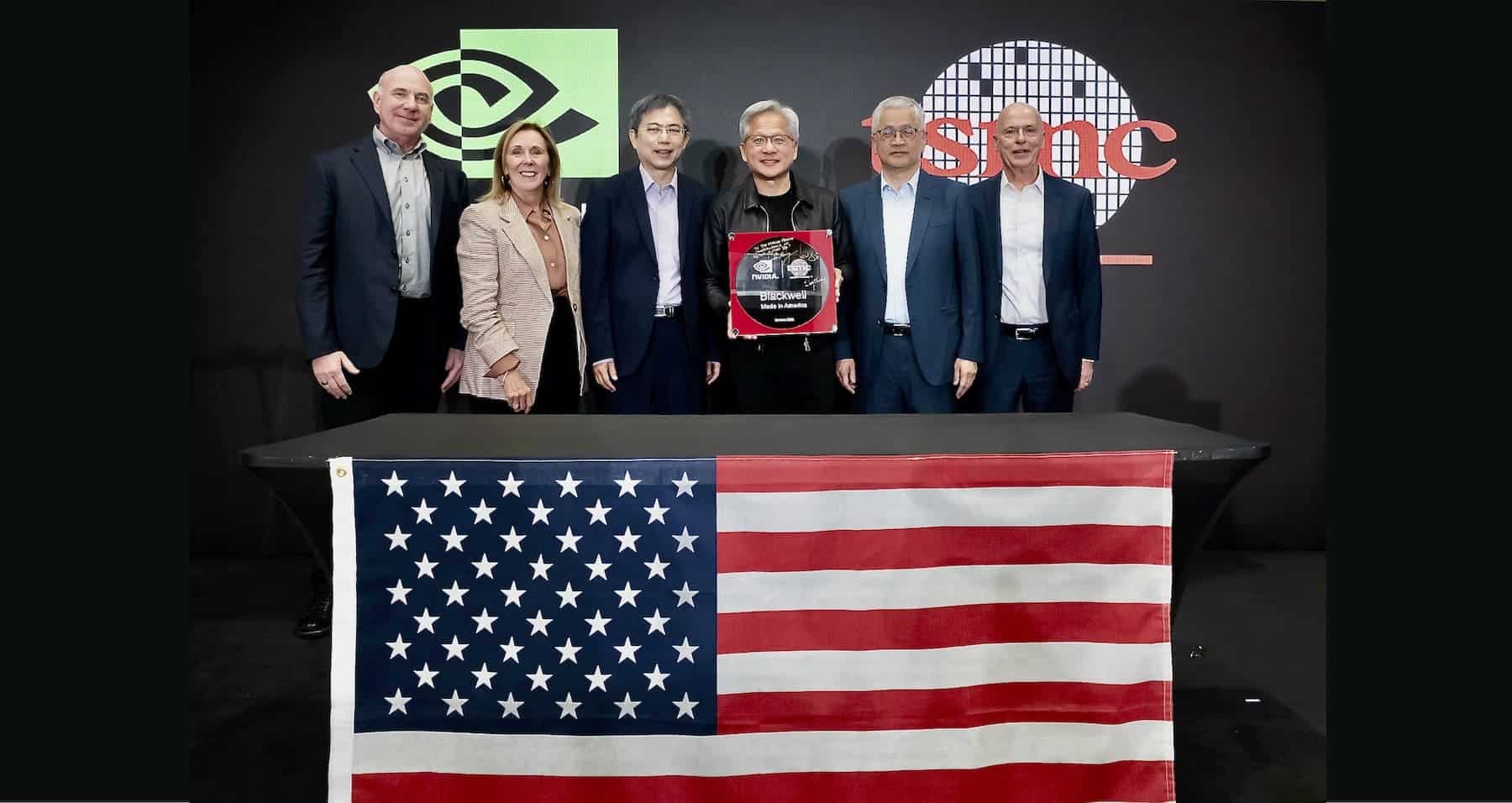
NVIDIA and TSMC have marked a symbolic and operational milestone for the semiconductor industry in the United States: the first Blackwell wafer produced on U.S. soil, specifically at the TSMC Arizona plant in Phoenix. The event, attended by NVIDIA founder and CEO Jensen Huang and TSMC executives, was seen as a clear signal that Blackwell is moving into full production and that part of the AI chip manufacturing stack is being internalized on American ground.
Beyond the photo op, this gesture fits into a narrative of technological reindustrialization: building a supply chain of advanced chips that reduces external dependencies and can meet the surging demand from AI data centers. NVIDIA framing this as a crucial step for “onshoring” critical capabilities: from the wafer fabrication process to plant operations incorporating robotics, digital twins, and in-house AI technologies.
What does it really mean to manufacture the first wafer?
In semiconductors, a wafer is just the beginning of a complex journey: after its fabrication, it undergoes dozens of deposition, patterning, , and dicing steps before transforming into functional integrated circuits. However, producing the first Blackwell wafer in the U.S. is significant because it indicates that process flows, materials, and equipment are calibrated for this architecture at the Arizona line, and that the program has shifted from pre-production to mass volume.
TSMC Arizona: advanced nodes and roadmap
The Phoenix site is set to produce advanced technologies at 2, 3, and 4 nanometers, plus A16, with applications spanning from AI to telecommunications and high-performance computing. This range of nodes sends two messages: first, that the factory is built with cutting-edge ambitions; second, that installed capacity will be scaled up to achieve latest-generation processes as materials, lithography, and the supply ecosystem mature.
A milestone laden with symbolism… and operations
During the ceremony, Jensen Huang and TSMC leaders sealed the Blackwell wafer. This act underscores the collaboration between a chip designer leading AI acceleration and the world’s largest contract manufacturer. Both emphasized that manufacturing in the U.S. enhances resilience in the supply chain and reduces logistical distances for the North American market, especially as GPU delivery timelines are a key competitive factor for hyperscalers, companies, and governments.
The story extends beyond wafer production. NVIDIA plans to deploy its advanced AI, robotics, and digital twins in new U.S. facilities to design and operate plants with greater predictability, visibility, and efficiency. Essentially, it involves applying the same automation and simulation approach to manufacturing that the company advocates for the industry at large.
What does Blackwell bring to AI’s future?
The Blackwell family, since its announcement, has been positioned as a leap in performance, energy efficiency, and return on investment—particularly in inference—compared to previous generations. In a market where scaling models and serving them in production demands power density, cost-effectiveness, and low latency, these variables determine where data center capex is invested. The fact that Blackwell reaches volume with part of its supply “made in USA” reinforces its appeal to clients seeking predictability and geographic resilience.
Why does this matter for the AI supply chain?
Localized manufacturing doesn’t immediately replace the capacity of TSMC and other providers outside the U.S., but it adds another hub with advanced capabilities. For end users, this can translate into:
- More predictable timelines for projects targeting North America.
- Reduced exposure to cross-oceanic logistical and regulatory risks.
- Improved coordination among design, manufacturing, and future plant operations supported by digital twins and NVIDIA robotics.
In other words: if hardware is the “engine” powering AI, having part of that engine close to the primary market accelerates the entire chain from wafer to rack.
Industrial and political context
The core message is that chip manufacturing is this century’s strategic industry. The focus on reindustrialization and bringing critical manufacturing back for security, employment, and technological leadership is evident. Amid the expansion of multi-megawatt AI campuses, governments have placed semiconductors at the forefront of industrial policy. The Arizona milestone aligns with this direction: investment, high-skilled jobs, and cutting-edge technology to sustain the AI era.
The key question for clients: what changes tomorrow?
For CIOs and platform teams, headlines matter, but what truly counts is what materializes in timelines and capacity:
- Mass production of Blackwell: improved visibility into delivery schedules over the coming quarters.
- Advanced nodes (2, 3, 4 nm) and A16 on the roadmap: technological foundation for better performance per watt.
- Operational technologies (AI, robotics, digital twins) applied to new plants: potential for efficiency and quality improvements, impacting supply stability.
The other critical variable is how the ramp unfolds: number of batches, product mix, and potential factory bottlenecks (materials, advanced packaging, memory) that could influence the pace.
Next stop: GTC Washington, D.C. (October 27–29)
The company will leverage the NVIDIA GTC in Washington, D.C. to expand its narrative and showcase use cases: enterprises, government agencies, research institutions, and startups leveraging its platform to accelerate projects. Expect to see practical examples around Blackwell, software, and the ecosystem translating the roadmap into real applications.
A perspective for tech media
This announcement is more than a snapshot. It carries three operational messages:
- Blackwell has moved from promise to production, with some of the volume manufactured in the U.S.
- TSMC Arizona is designed to target advanced nodes —2, 3, and 4 nm, plus A16— which are essential for AI, telecom, and HPC.
- NVIDIA aims to industrialize its own manufacturing approach: using AI, robotics, and digital twins to design and operate plants in the U.S., closing the loop on technology applied to manufacturing.
How everything fits into actual timelines and product mixes remains to be seen, but the trajectory is clear: more capacity, closer to the primary market, with an architecture —Blackwell— born to serve the explosion of generative AI and scalable inference.
Frequently Asked Questions
What exactly was announced in Arizona regarding Blackwell?
The first Blackwell wafer produced in the U.S. by TSMC in Phoenix, indicating that Blackwell is entering volume production with part of the manufacturing process onshore.
What technologies will TSMC Arizona produce, and what are their applications?
It will manufacture advanced chips at 2, 3, and 4 nanometers, plus A16, vital for AI, telecoms, and high-performance computing.
What practical benefits does U.S. manufacturing offer customers?
Increased resilience and predictability in the North American supply chain, shorter lead times, and better alignment between design, manufacturing, and plant operation, supported by AI and robotics.
When will more product details and use cases be available?
During NVIDIA GTC in Washington, D.C. (October 27–29), where the company typically showcases software, tools, and references translating its roadmap into tangible projects.
via: blogs.nvidia