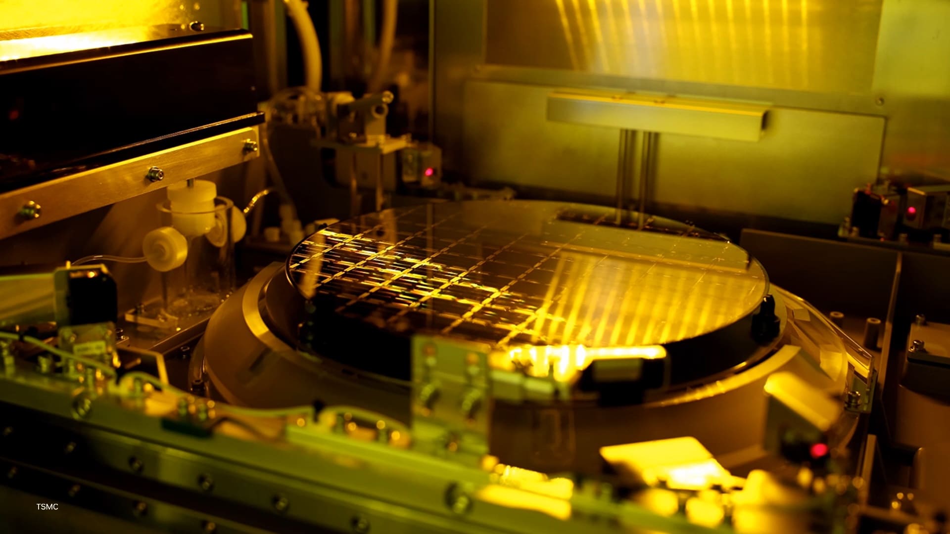
NVIDIA and TSMC have announced a collaboration that brings artificial intelligence and accelerated computing to one of the most complex parts of the tech industry: advanced semiconductor manufacturing. Unveiled at GTC Taipei, the partnership goes beyond designing more powerful chips; it aims to integrate AI models, CUDA-X libraries, computer vision, and digital simulation directly within TSMC’s factories.
This move sends an important signal across the industry. As chips grow smaller and designs denser, taking a processor from concept to volume production has become an enormous computational challenge. Computational lithography, transistor simulations, process control, wafer inspection, and modern fab planning generate workloads that can no longer rely solely on traditional methods.
TSMC, the world’s largest contract semiconductor manufacturer, is leveraging NVIDIA technologies to shorten cycle times, improve energy efficiency, increase operational productivity, and enhance the performance of its advanced manufacturing processes. In practice, AI is no longer just a burden running on chips produced by TSMC; it’s also a tool helping to manufacture those same chips.
CUDA-X enters lithography, simulation, and process control
A core element of the announcement is the use of CUDA-X libraries and AI models to accelerate critical tasks within the design and manufacturing cycle. NVIDIA highlights four key areas: computational lithography, transistor and material simulation, advanced process control, and factory operation optimization.
In computational lithography, TSMC is using NVIDIA cuLitho, a GPU-accelerated library designed for mask design tasks. NVIDIA states this technology offers an improvement of 20% to 50% in cost-effectiveness or cycle time compared to CPU-based approaches, while maintaining the same total cost of ownership. In an industry where reducing cycle time can accelerate node launches or increase capacity, this margin is significant.
Simulation also gains importance. TSMC employs NVIDIA cuEST, a GPU-accelerated library for electronic structure simulation, which NVIDIA claims can deliver chemical simulations up to 50 times faster on average for semiconductor material design. Such workloads are critical when exploring new materials, interfaces, and physical behaviors affecting transistor performance and reliability.
For advanced process control, TSMC uses NVIDIA cuML to accelerate large-scale analytics on GPUs. The goal is to process hundreds of thousands of parameters scattered across thousands of manufacturing steps, converting them into accurate inputs for machine learning models. This aims to reduce process variations—a major focus for any advanced chip manufacturer, since tiny deviations can impact performance or yield.
The fourth area involves factory operational optimization. NVIDIA notes that using CUDA and H200 GPUs has improved production scheduling and the management of complex constraints within fabs. Semiconductor plant planning is no trivial matter: equipment, materials, robots, shifts, maintenance, customer priorities, and process routes must be coordinated with high precision.
Artificial vision for nanometric defect detection
Defect inspection is another critical front. As chips become more complex, even tiny irregularities can affect final quality. TSMC is utilizing NVIDIA Metropolis and NVIDIA TAO Toolkit to enhance advanced defect classification with artificial vision.
The advantage lies not just in detecting more defects but in reducing the need to label and retrain models repeatedly as process conditions, inspection tools, or defect types change. In a cutting-edge fab, failure patterns can vary and evolve. If vision systems require extensive manual upkeep to stay current, automation’s value diminishes.
AI applied to inspection helps bridge this gap. A system capable of detecting nanometric defects, learning pattern changes, and supporting quality teams enables earlier reactions and improved manufacturing yield. For TSMC, this is especially critical since their clients depend on tight volumes, schedules, and yields for AI chips, mobile, server, automotive, and advanced electronics applications.
FabTwin: virtual factory before physical construction
NVIDIA has also highlighted TSMC’s use of Omniverse to explore FabTwin, a virtual factory environment designed to evaluate tool layouts and simulation flows before making physical changes or large capital investments.
An advanced fab is one of the most complex industrial facilities. It combines extremely expensive manufacturing tools, vacuum systems, cleanrooms, robots, personnel, wafer transport, environmental controls, chemistry, energy, cooling, and planning software. A layout design error can impact productivity, maintenance, safety, or expansion capacity.
A digital twin allows comparison of configurations, early detection of constraints, analysis of material flows, and faster decision-making. It doesn’t replace physical engineering but reduces uncertainty and improves planning. With the surging demand for AI chips, any advance that enables building or expanding capacity more confidently holds strategic value.
AI as a tool to manufacture the next generation of AI chips
The collaboration between NVIDIA and TSMC illustrates an increasingly evident circularity: AI needs more powerful chips; these chips require even more advanced fabs; and those fabs are beginning to rely on AI for higher precision, speed, and efficiency. The frontier now extends beyond designing faster GPUs to improving every process layer involved in their production.
NVIDIA founder and CEO Jensen Huang explained that TSMC is bringing AI and accelerated computing “inside the fab” to address design and manufacturing challenges through simulation, optimization, and intelligent automation. C.C. Wei, TSMC’s President and CEO, framed the partnership as part of a long-standing relationship aimed at strengthening technological leadership and manufacturing excellence.
The alliance also shows how NVIDIA is expanding its role beyond data centers. Its GPUs and libraries are now central to model training and inference, but now they also underpin lithography, simulation, inspection, and industrial management tools. For TSMC, integrating these capabilities could help sustain its leadership in advanced chip manufacturing, especially as AI demand requires more capacity, precision, and faster innovation cycles.
The semiconductor industry has long relied on coordinated advances across design, materials, lithography, packaging, software, and fabrication. Now, AI is starting to act as a cross-cutting layer across all stages. If the promise is fulfilled, future fabs will not only produce chips for AI but will also be managed, simulated, and optimized with AI integrated at every level.
Frequently Asked Questions
What did NVIDIA and TSMC announce?
They announced that TSMC is leveraging NVIDIA’s accelerated computing and AI to enhance semiconductor design and manufacturing processes, from lithography and simulation to inspection and factory operations.
What is NVIDIA cuLitho?
cuLitho is a GPU-accelerated library for computational lithography. According to NVIDIA, it improves cost-effectiveness or cycle time by 20% to 50% over CPU-based methods.
How does TSMC use NVIDIA Metropolis and TAO Toolkit?
TSMC employs them for advancing automated defect inspection with AI vision, improving nanometric defect detection and reducing manual labeling and retraining needs.
What is FabTwin?
FabTwin is a virtual factory environment that TSMC is exploring with NVIDIA Omniverse libraries to evaluate layouts, tools, and simulation workflows before making physical changes or investments.
via: nvidianews.nvidia