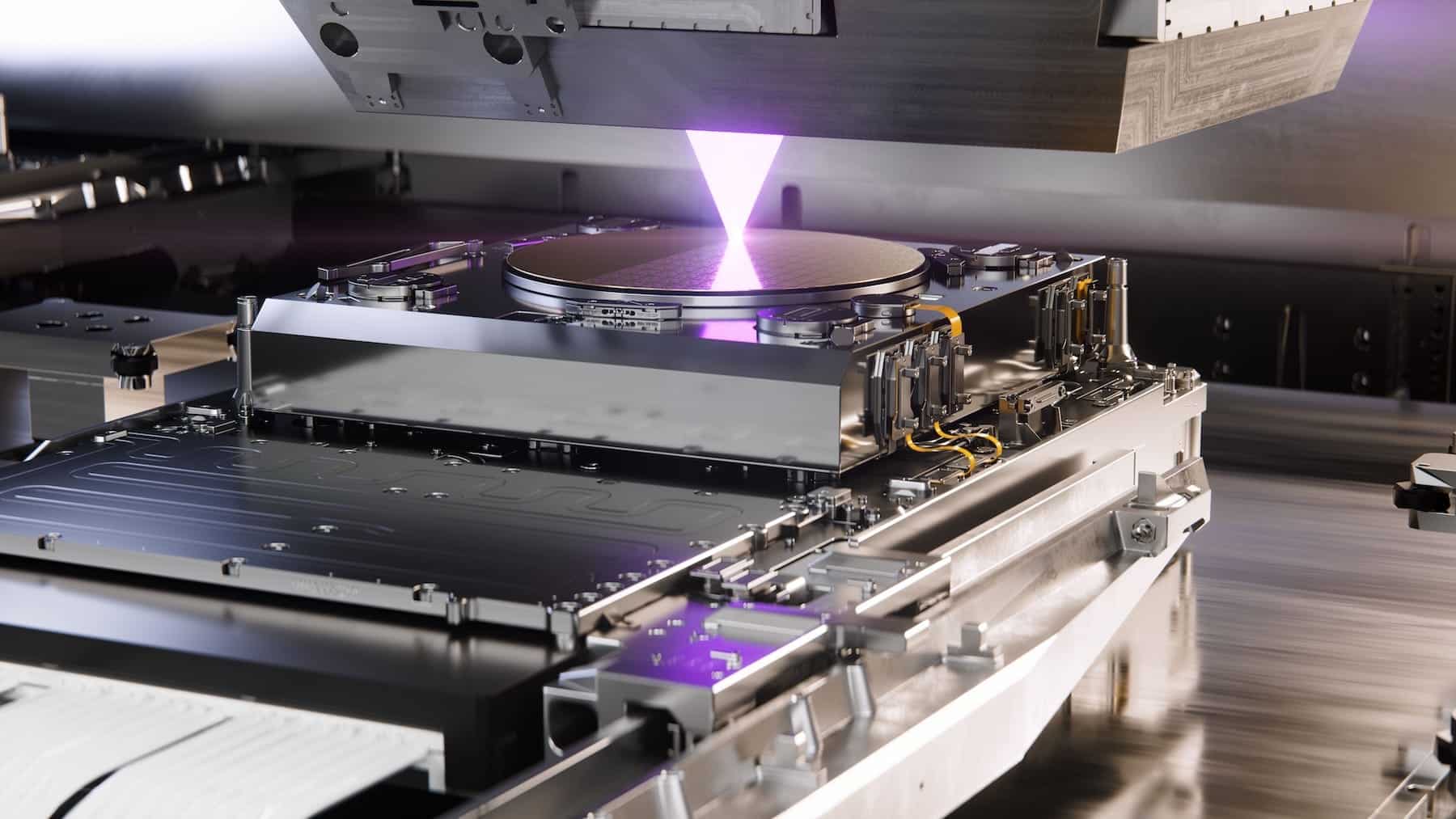
Nikon aims to regain ground in one of the most challenging markets in the tech industry: semiconductor lithography. The Japanese company, better known by the general public for its cameras, is preparing a commercial offensive based on lower prices for its ArF equipment, a deep ultraviolet lithography technology that remains essential even in advanced chip fabrication plants.
This move was explained by Yasuhiro Ohmura, the new president and CEO of Nikon since April, in an interview with Nikkei Asia. According to information gathered by various tech media outlets, Nikon is in talks with major chip manufacturers in the US and Asia for new orders of ArF tools, with negotiations close to turning into purchase commitments. The strategy is clear: compete with ASML not in EUV, where the Dutch company maintains a near-absolute position, but in a segment of the market where there is still room to press on price, compatibility, and supply alternatives.
Not EUV, but still critical lithography
Precision is key in this story. Nikon will not break ASML’s monopoly on EUV lithography, the extreme ultraviolet technology used at the most advanced nodes. Nikon itself abandoned that race years ago, while ASML has succeeded in turning EUV into a technological barrier almost impossible to replicate in the short term. The Japanese offensive focuses on ArF immersion, a mature DUV (deep ultraviolet) technology still very much needed.
This nuance changes the perspective. EUV lithography makes headlines because it enables the production of cutting-edge chips, but many layers in an advanced chip are still manufactured with DUV methods, including ArF immersion tools. These systems are also used in memory, logic, sensors, automotive chips, industrial electronics, and mature nodes that remain vital to the digital economy.
ASML closed 2025 with net sales of €32.7 billion and reported the sale of 535 systems: 48 EUV, 279 DUV, and 208 metrology and inspection systems, according to its annual report. This data helps explain why the battle isn’t limited to the most advanced lithography segment. DUV volume remains substantial and underpins a central part of the semiconductor equipment business.
Nikon is trying to enter precisely there. The company argues that its higher degree of internal component integration gives it a competitive edge on cost. Ohmura summarized it simply: Nikon manufactures many parts in-house, which would give it an advantage in a price war. If chip manufacturers want to reduce dependence on ASML and keep costs down for their lines, having a second viable supplier can be attractive.
| Technology | Role in Chip Manufacturing | Competitive Position |
|---|---|---|
| EUV | Most advanced nodes and critical layers | Practically exclusive domain of ASML |
| DUV ArF immersion | Many layers in advanced and mature nodes | ASML leads, but Nikon seeks to regain ground |
| KrF and i-line | Mature nodes, sensors, power, and other uses | More diversified market |
| Nanoimprint | Alternative explored by Canon | Promising technology, still limited adoption |
Nikon needs to win back clients
This strategy comes after a very tough period for Nikon in semiconductor lithography. TrendForce, citing Nikon data and other industry reports, indicated that the company sold 11 ArF systems in its fiscal year closed in March 2024, but registered no ArF sales in the first three quarters of fiscal 2025. The same source estimated that ASML’s market share in lithography is around 90%.
Nikon’s own financial documents reflect this pressure. In February 2025, the company projected a decline in revenue from its Precision Equipment segment due to lower ArF system sales, although it expected to partly offset this with lithography equipment for FPD displays. In that same presentation, Nikon confirmed the development of a new ArF immersion platform with a new lens, a new wafer stage, and compatibility with systems from other companies, with a prototype delivery expected in fiscal year 2028.
That compatibility is one of the most important aspects. For a chip maker, switching lithography providers isn’t like replacing a printer. fabs are designed around processes, masks, recipes, maintenance, training, metrology, and operational data accumulated over years. If Nikon wants to become a real option again, its tools need to fit into lines where ASML is already in place, where any interruption could cost millions.
It seems the company has understood this challenge. Its new ArF platform aims to better integrate into processes where customers already use ASML equipment. If it also comes at a lower price, Nikon could position itself as a way to diversify risk, cut costs, and increase capacity in a market under pressure from demands for AI, advanced memory, and new factories.
Price can open doors, but it’s not enough
The semiconductor industry doesn’t buy solely based on price. Reliability, productivity, service availability, throughput per wafer, process stability, and trust built over time are all critical factors. ASML’s dominance isn’t accidental. It has cultivated decades-long relationships with TSMC, Samsung, Intel, SK hynix, Micron, and other major manufacturers, along with a supply chain difficult to match.
That’s the challenge for Nikon. A cheaper system can be attractive, but the real costs in a fab are not measured only by purchase price. If a tool has lower availability, requires more maintenance, yields less process data, or presents greater integration risks, the initial savings can evaporate. Demonstrating performance in real-world clients will be key, not just presenting a paper alternative.
The situation with Intel also weighs heavily. For years, Intel was one of Nikon’s most important ArF customers, according to info cited by Tom’s Hardware. But the US company has reduced investment and is experiencing a challenging phase in manufacturing, forcing Nikon to seek a broader customer base.
Demand could play in Nikon’s favor. AI is accelerating investments in memory, advanced packaging, specialized chips, and additional capacity. While much focus is on GPUs and accelerators, there are factories behind these that still require many DUV tools. Plus, manufacturers prefer to avoid dependency on a single supplier if a credible alternative exists.
A sign of fragmentation in the semiconductor supply chain
Nikon’s offensive also fits into a broader geopolitical context. The US, Europe, Japan, Taiwan, South Korea, and China are strengthening their chip supply chains. Lithography remains one of the most sensitive bottlenecks. In EUV, ASML’s position will remain tough to challenge. In DUV, there may be more room for competition, aggressive pricing, and diversification strategies.
Japan has long sought to regain influence in semiconductors. Nikon, Canon, Tokyo Electron, Lasertec, SCREEN, and other Japanese suppliers hold significant capabilities in equipment, materials, optics, inspection, and processes. Canon has pushed its nanoimprint technology as an alternative for certain applications, while Nikon is trying to re-engage with the ArF market through a more affordable, compatible platform.
This move doesn’t guarantee Nikon’s triumphant return. The company starts from a weakened position, with low ArF sales and the need to rebuild trust. But its strategy touches on a critical industry point: chip manufacturing costs have skyrocketed, demand for tools is growing, and ASML’s dominant position makes many customers see value in maintaining a second supplier.
The battle won’t be to overthrow ASML in EUV. It will be for a less visible but highly profitable and essential part of modern manufacturing. If Nikon can deliver reliable, compatible, and significantly cheaper ArF equipment, it might reclaim some ground. Failing that, industry talk will continue to focus on diversification, with many still choosing to buy from the provider already in control.
Frequently Asked Questions
Can Nikon break ASML’s EUV monopoly?
No. Nikon’s strategy concentrates on ArF immersion tools within DUV lithography. ASML maintains a nearly exclusive position in EUV.
Why is ArF lithography still important?
Because many layers in advanced chips and a large portion of mature nodes still rely on DUV ArF tools, even when some critical layers are made with EUV.
What does Nikon aim to offer against ASML?
Lower prices, internally manufactured components, and a new ArF platform compatible with tools already installed in fabs using ASML systems.
When will Nikon’s new ArF platform be available?
Nikon has indicated in financial documents that it plans to deliver a prototype of its new ArF immersion platform in fiscal year 2028.
via: Nikkei