The race for memory for AI is no longer limited to squeezing HBM or stacking layers in NAND. Another approach has begun to take shape—one that for years sounded more like a lab promise than an industrial roadmap: 3D DRAM. In this field, NEO Semiconductor has just taken a notable step. The company announced promising results from a silicon proof of concept for its 3D X-DRAM technology, along with a new strategic investment led by Stan Shih, founder of Acer and former TSMC board member for over two decades.
Here, the significance isn’t just the corporate headline but what the announcement implies. NEO claims its 3D X-DRAM has demonstrated it can be manufactured using already mature 3D NAND infrastructure, including existing equipment, materials, and processes. In an industry where the cost of bringing a new memory to production is often nearly as critical as the theoretical performance, this point is arguably the most relevant part of the message. The company isn’t saying it already has a commercial 3D DRAM ready for market, but it has validated in silicon an architecture that aims to leverage part of the industrial ecosystem already built around vertical NAND.
The publicly shared proof of concept results are, on paper, impressive. NEO reports achieving a read/write latency under 10 nanoseconds, data retention over one second at 85°C, resistance to disturbances on bit-line and word-line longer than a second at that temperature, and a endurance exceeding 10^14 cycles. The company compares this retention to the 64 milliseconds standard used in conventional DRAM, claiming it to be about 15 times better. It’s important to note that these figures come from the company itself and pertain to a proof of concept, not a scaled commercial product.
Why this announcement matters beyond marketing
Traditional DRAM remains essential but has been approaching increasingly challenging physical and economic limits. NEO’s own statement includes insights from Jeongdong Choe, Senior Technical Fellow and SVP at TechInsights, who places this development within a broader industry trend toward 3D architectures and novel memory cells to meet AI workloads and data-centric systems. That is, NEO isn’t alone in exploring this path, but it aims to position itself among the first companies to translate the concept from simulation to actual silicon.
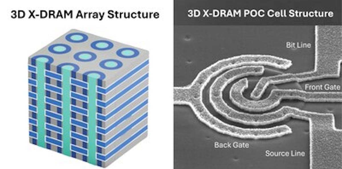
Indeed, the company has been building this technical narrative for several years. In May 2023, it first introduced its 3D X-DRAM as a “NAND-like” architecture designed to break through the capacity bottleneck of conventional DRAM. Later, in May 2025, NEO evolved the idea with a version based on IGZO and mentioned densities of up to 512 Gb and retention times of 450 seconds, emphasizing that the process remains compatible with 3D NAND technology. That phase was still clearly pre-commercial; the current breakthrough is that the company now claims to have moved from promising simulation to a physical fabrication and evaluation.
This transition is further supported by a strong Taiwanese foundation. NEO explains that the proof of concept was developed in collaboration with the National Yang Ming Chiao Tung University (NYCU), specifically through its Industry-Academia Innovation School, with fabrication and testing performed at the Taiwan Semiconductor Research Institute (NIAR-TSRI). According to the release, both the academic institution and the research institute confirm the device surpassed electrical and reliability assessments, boosting credibility—though it remains a first-phase validation.
Less data movement, more density, and a new potential path for AI memory
NEO’s core thesis is clear: if a vertical DRAM can be built using existing machinery, materials, and processes derived from the 3D NAND universe, the industry could unlock new avenues to scale density, energy efficiency, and cost in the era of AI. The company explicitly mentions applications for AI systems and data-centric computing, proposing 3D X-DRAM as a foundational technology for future high-density memories, including their X-HBM and 3D X-AI families. It’s no coincidence that their most recent roadmap already seeks to unify these components under a common technological umbrella.
Nonetheless, maintaining a realistic perspective is crucial. A successful proof of concept does not equate to immediate industrial adoption. Between a POC and deploying memory in AI servers, many stages remain: array-level implementation, development of multi-layer test chips, cost validation, packaging, integration with controllers, and, importantly, a manufacturing partner capable of large-scale production. NEO acknowledges that the next phase will focus on array-level implementation, developing multi-layer test chips, and strengthening conversations with leading memory and semiconductor companies.
The involvement of Stan Shih at this stage also carries strategic significance. Beyond funding, his profile contributes industrial legitimacy and connections within Taiwan’s tech ecosystem—an element that could be decisive for a technology that requires more than just a good patent to thrive. According to the company, Shih leads the new investor group backing the next phase of the project.
A serious advance, but still in the development stage
Therefore, this news deserves attention but not premature celebration. NEO has not, by itself, solved the future of AI memory, but it has demonstrated a signal the industry has been waiting for: that 3D DRAM might begin to emerge from simulation and prototype stages into tangible fabrication with promising initial metrics. If they can turn this proof of concept into a credible industrial roadmap, it could open a highly relevant pathway, especially as demand for AI memory continues to grow and traditional DRAM scalability faces increasing challenges.
Frequently Asked Questions
What has NEO Semiconductor announced exactly?
NEO announced promising results from a silicon proof of concept for its 3D X-DRAM technology and a new strategic investment led by Stan Shih to support the next development phase.
What technical figures has the company provided?
The company reports latency under 10 ns, retention over 1 second at 85°C, resistance to line and word-line disturbances, and an endurance over 10^14 cycles. These results come from NEO’s own testing within the proof of concept.
Is 3D X-DRAM ready for commercial production?
No. NEO has validated a proof of concept and now plans to move toward array implementation, multi-layer chips, and partnerships with memory and semiconductor manufacturers.
Why could this technology be important for AI?
Because NEO envisions a higher density and potentially more efficient memory, supported by mature 3D NAND processes, which could help address capacity and cost challenges for future AI systems.
via: prnewswire