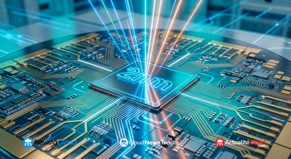
Elon Musk has once again placed the semiconductor industry at the center of public debate with a provocative and unlikely statement: he claims that when Tesla builds a factory capable of producing 2-nanometer chips, he will be able to walk in and “grab a hamburger” and “smoke a cigar” inside the plant. The remark, made during a conversation on the Moonshots podcast, has been interpreted as a direct critique of how the sector designs and operates cleanrooms, the heart of any advanced wafer manufacturing facility.
Musk argued that “cleanrooms are being mismanaged” in modern factories and defended that the key lies in keeping the wafers “isolated” throughout the entire process. In his view, contamination control should not rely so much on humans becoming a “risk” (suits, strict protocols, restricted zones), but rather on ensuring that the product remains encapsulated and protected continuously.

In any case, the statement has not been read as a technical manual — nor as a detailed plan — but as a mix of challenge, marketing, and frustration with the reality of a market where manufacturing cutting-edge chips has become a global bottleneck. And, incidentally, as a way to highlight that Tesla aims to play a more ambitious role in the silicon supply chain.
The obsession with control… and the clash with physics
The industry does not build cleanrooms on a whim. A modern semiconductor plant is, in fact, a massive industrial ecosystem: ultra-controlled production areas, lower-level “subfabs” with vacuum pumps, gases, ventilation, and extraction systems, service corridors for tool maintenance, and infrastructure for chemicals and waste management designed to operate with zero margin for error. In such an environment, contamination not only reduces chip yield; it can also damage highly sensitive and expensive equipment.
This is where Musk’s comment clashes with reality. Although wafer isolation exists — and is part of daily operations in modern factories — it does not eliminate the need for environment control: interactions with tools, materials, optics, and processes still occur within a context that demands extraordinary cleanliness levels. Smoke, organic particles, and food residues are not mere “nuisances”: they are precisely what industrial protocols aim to prevent because they affect the process and, in advanced scenarios, the equipment itself.
The idea of “flipping” the cleanrooms also oversimplifies a key point: even if wafers are transported in containers and handled automatically, state-of-the-art fabs are designed to protect not just the chip, but the entire manufacturing environment. In advanced lithography, for example, material stability, chemical purity, and absence of contaminants are non-negotiable. The industry strictly restricts food and tobacco in production areas for contamination and safety reasons.
Tesla and the dream of chip manufacturing: from “Terafab” to foundry partnerships
The context surrounding these statements helps explain why they are surfacing now. Tesla is not unrelated to semiconductors: it designs chips for its vehicles and pursues an AI strategy linked to autonomous driving and robotics. Musk had previously hinted that by 2025, the company’s demand for chips could lead to a radical solution: a “Terafab,” an even larger concept than the “Giga fabs” used to describe major manufacturing complexes.
But building a factory capable of competing at 2 nm is not comparable to setting up a conventional production line. It’s a technical, financial, and talent-intensive gamble that usually only industry giants undertake. In fact, Jensen Huang (NVIDIA) himself publicly emphasized that manufacturing advanced chips is “extremely difficult,” not only because of constructing the facility but also due to the engineering and accumulated knowledge involved in the process.
Meanwhile, Tesla is working within a more realistic sphere: collaborating with established manufacturers. Musk has spoken about relationships with partners like TSMC and Samsung, and the company has been linked to agreements to secure supply and capacity. This is a clear signal that — in the short to medium term — the practical approach remains dependent on established foundries, rather than replacing them.
Provocation or a sign of an emerging trend?
Although the image of a “2 nm factory” with a cigar and a hamburger may seem to be designed for headlines, it does touch on a real debate: the industry has been moving toward more isolated mini-environments, increased automation, and greater process containment to reduce human risk over the years. In other words, Musk’s intuition about “more isolation” is not entirely divorced from technological evolution. The issue is that this path does not eliminate the need for cleanrooms; it adds additional layers of control.
Ultimately, the message conveys an idea Musk often repeats in different contexts: if a system seems too rigid, it can probably be redesigned. In semiconductors, however, rigidity is not cultural but physical. And at 2 nm, physics usually has the final say.
Frequently Asked Questions
What does “2 nm” really mean in chips, and why is it so difficult to manufacture them?
It’s a commercial label associated with cutting-edge fabrication nodes. It involves extremely complex processes, costly equipment, and minimal tolerances, with strict control over variability and contamination.
Can advanced chips be made without cleanrooms if wafers are “isolated”?
The industry already uses containment and automation, but still requires ultra-controlled environments: not only for wafers but also for sensitive equipment, materials, and processes.
How much does it cost to build a cutting-edge semiconductor factory?
Figures typically run into tens of billions of dollars, plus years of construction and a specialized supply chain (equipment, chemicals, personnel, and industrial software).
Could Tesla become a chip manufacturer like TSMC or Samsung?
Today, Tesla mainly acts as a designer and capacity purchaser. Building and operating a leading-edge foundry is a complexity leap that few companies have achieved.