The seventh generation of Google’s artificial intelligence accelerators has a name and silicon: TPU v7 Ironwood. Designed to compete toe-to-toe with NVIDIA’s Blackwell GPUs in large-scale inference workloads, this new family of chips is not only a strategic move for Google Cloud. It also represents a multimillion-dollar opportunity for MediaTek, which collaborated on the design and is now looking to transfer some of that expertise to its upcoming high-end mobile SoC, the Dimensity 9600.
Ironwood: the TPU Google aims to challenge NVIDIA with
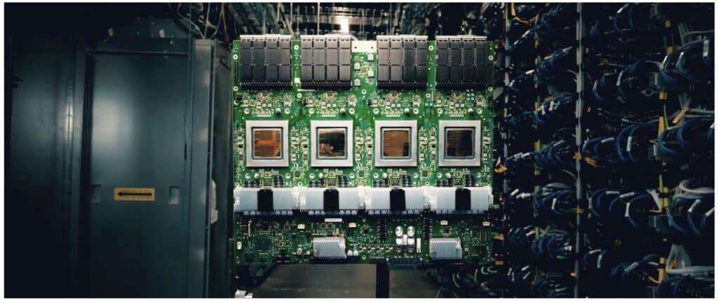
Ironwood is Google’s seventh-generation TPU and is designed for training and inference of massive models, both dense and Mixture-of-Experts. Each chip TPU7x includes:
- Two TensorCores for matrix computation (including FP8) and
- Four SparseCores, optimized for working with sparse structures like embeddings, commonly used in language models.
- 192 GiB of HBM3E memory per chip, with an almost 7.4 TB/s bandwidth.
The architecture adopts a dual-chiplet design: each physical chip is divided into two “logical devices,” each with its own TensorCore, SparseCores, and 96 GiB of HBM. The two halves communicate via a die-to-die link that is up to 6 times faster than traditional chip interconnects (ICI).
At the system level, Google scales these chips into extreme configurations:
- 64 chips form a basic TPU “cube,” interconnected with 1.2 TB/s of bidirectional bandwidth per chip.
- Multiple cubes connect through an Optical Circuit Switching (OCS) network to create a superpod of 9,216 chips, with approximately 42.5 exaFLOPS FP8 and 1.77 PB of shared HBM.
With these capabilities, Ironwood closes much of the gap in compute power, memory, and bandwidth compared to NVIDIA’s GB200/GB300 platform, and does so with a very aggressive focus on energy efficiency and total cost of ownership (TCO) for inference—the fastest-growing segment in the cloud.
MediaTek’s role: from Ironwood I/O to mobile SoC design
The most intriguing part of this story for the mobile industry is who helped Google build this monster. Unlike previous generations, where Broadcom was the key design partner, several reports point to Google relying on MediaTek to design Ironwood’s input/output (I/O) modules, which handle communication between the chip and the rest of the system.
This move has several implications:
- Strategic partner shift: Google diversifies away from Broadcom and turns to a provider with extensive experience in consumer SoCs, where performance versus power consumption is critical.
- Reusability of expertise: Although a data center TPU and a mobile SoC are very different architectures, the design of high-speed I/O, power management, and advanced packaging share fundamental challenges.
- Direct economic impact: UBS estimates that MediaTek could earn around $4 billion thanks to its collaboration with Google on this seventh generation of TPUs.
For MediaTek, this isn’t just an additional AI revenue line for data centers—it’s a high-profile testing ground to improve the efficiency of their future mobile chipsets, especially as the company has committed to aggressive performance targets.
Dimensity 9600: a flagship that demands every milliwatt of efficiency
The Dimensity 9600 will be MediaTek’s upcoming flagship for high-end 5G smartphones. Leaks suggest it will launch in 2026 as a processor built on one of TSMC’s most advanced nodes, with performance expected to fall between Qualcomm’s Snapdragon 8 Elite Gen 6 “regular” and the Pro version.
Meanwhile, the company has taken a risky strategy: with the Dimensity 9300 and 9500, it already abandoned traditional efficiency cores, opting for configurations with only large cores (big cores), sparking debate about their real-world power consumption over prolonged use.
In this context, any gains in energy management are crucial. This is where the lessons from Ironwood come into play:
- More aggressive power gating
Designing I/O for a TPU that moves terabytes per second of HBM forces pushing the limits of selective block shutdown when idle. MediaTek can apply these techniques to the Dimensity 9600 to turn off controllers, buses, and peripherals more granularly, reducing idle and light-load power. - Enhanced voltage scaling
Ironwood operates with highly optimized voltage margins to maximize efficiency in FP8 and BF16. Fine-tuning voltage regulation algorithms in the Dimensity 9600—for instance, through more precise DVFS curves—can help the SoC run at peak efficiency for longer periods. - Refined clock-gating
Experience optimizing clock routes in a high-density TPU can be reused to reduce clock activity where no performance benefit is gained. In a mobile SoC without efficiency cores, the ability to “slow down” whole blocks when not needed is key to preserving battery life.
Sources like Wccftech emphasize that MediaTek can’t directly transfer everything learned from Ironwood to a smartphone processor, given the obvious differences between a data center ASIC and a flagship mobile AP. Still, there’s room for iterative improvements that could boost autonomy in comparison to Qualcomm and Apple.
AI in the cloud and on the device: two fronts, one battle
The collaboration between Google and MediaTek also illustrates how the AI value chain is evolving:
- In the cloud, Ironwood and Google’s TPUs compete to reduce inference token costs and boost performance per watt, aiming to challenge NVIDIA’s dominance in hyperscalers.
- On the device, the new Dimensity and Snapdragon chips compete to run generative models and local assistants with minimal impact on battery life and thermal performance.
MediaTek now operates on both fronts. Its work on Ironwood’s I/O modules places it at the forefront of ultra-scale AI data center development, while the Dimensity 9600 will showcase how much of that expertise can be distilled into a pocket-sized chip.
If these efficiency gains materialize, the end user won’t see “TPU v7” in their phone specifications, but they will notice more battery life, less throttling, and more sustainable local AI capabilities. In a market where everyone boasts TOPS and NPUs, the real edge might once again lie in something as fundamental as efficiency engineering.