
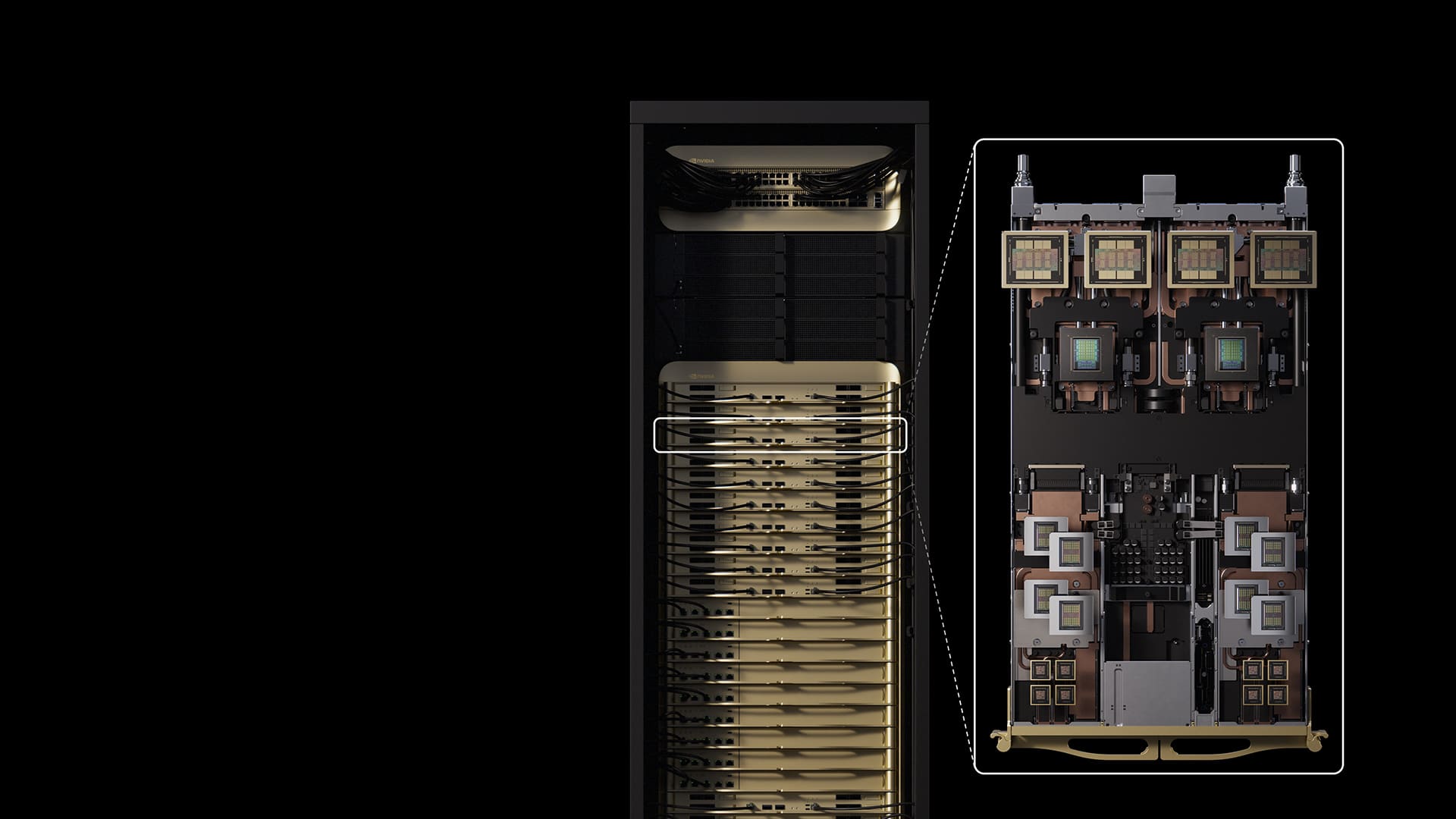
The trajectory of artificial intelligence is often described as a series of increasingly powerful chips. More FLOPS, more HBM memory, higher bandwidth, and more racks per data center. But the recent news surrounding NVIDIA points to a less glamorous and much more uncomfortable reality: the limit is not always in designing a larger GPU, but in connecting, powering, cooling, and manufacturing them at volume.
According to an analysis shared by SemiAnalysis, NVIDIA’s Kyber NVL144 architecture has experienced a significant delay and is now expected around 2028. Additionally, the alternative design NVL72x2, which aimed to place two Oberon racks back-to-back to extend copper scaling, has reportedly been canceled. NVIDIA has not officially confirmed this information, so it should be treated as supply chain and architecture speculation rather than an official announcement.
Nevertheless, the core issue remains highly relevant. NVIDIA had introduced Kyber as part of its evolution toward rack-scale and multi-rack AI systems. In its technical blog, the company described Kyber as an architecture capable of doubling NVLink’s domain per rack to up to 144 GPUs and serving as a foundation for even larger systems, such as NVL1152, utilizing direct optical interconnections between racks.
The problem is no longer just the chip
Over recent years, NVIDIA has established a formidable advantage not just with its GPUs but with the entire system ecosystem surrounding them. NVLink, NVSwitch, integrated racks, liquid cooling, Spectrum-X and InfiniBand networks, software, and a coordinated supply chain have enabled the sale of AI infrastructure as nearly complete blocks, rather than isolated accelerators.
This model works as long as the architecture can scale. The challenge appears when hundreds of GPUs need to operate as a single, coherent system with low latency and sufficient bandwidth. At that stage, copper traces, connectors, midplanes, cables, power consumption, and thermal dissipation become engineering priorities—not just details, but central to the product.
Kyber NVL144 was precisely aiming to expand this scaling domain. The idea was to increase the number of GPUs connected within an NVLink environment, reducing dependence on slower external networks for certain workloads. In generative AI, especially in training and inference of large models, this difference can impact token costs, GPU utilization, and data center efficiency.
The reported delay is attributed to the difficulty in reliably manufacturing the midplane PCB, a critical component for system interconnection. It’s not a minor fault. In these architectures, performance depends on high-speed signals traveling over tight physical distances. Engineering here becomes tangible: copper, fiber, heat, tolerances, maintenance, and assembly.
Rubin Ultra also adjusts its course
The news also follows another significant development: the alleged abandonment of the Rubin Ultra with four compute dies. Tom’s Hardware, citing SemiAnalysis, reported that NVIDIA had canceled this more ambitious version due to manufacturing challenges and opted for a configuration with two compute dies, which is easier to produce. They also noted that this information is unofficial and should be taken cautiously.
The difference is substantial. The four-die design promised to double the compute area compared to Rubin and to boost performance per package aggressively. Reducing it to two dies lowers industrial risk but also limits potential gains. In practice, NVIDIA might offset some of that loss by selling more racks or systems, but the message to the market changes: even the AI leader faces physical, packaging, and manufacturing limits.
This does not mean NVIDIA has lost its advantage. That would be an overstatement. The company maintains a dominant position in accelerators, software, networking, and ecosystem. However, it suggests that the margin of superiority could narrow during a phase where success depends not only on having the best GPU but on building the best complete system.
That is where AMD, Google, and major hyperscalers come into play. AMD has rack-scale solutions with Instinct MI500X and compatible CPUs slated for 2027, within an annual roadmap evolving CPUs, GPUs, and AI systems. Google, for its part, has separated its eighth-generation TPU into two specialized architectures: TPU 8t for training and TPU 8i for inference, emphasizing efficiency, scalability, and client-specific workloads.
The opportunity for these competitors lies not in NVIDIA disappearing but in the slight delays in NVIDIA’s scaling dominance creating room for alternative architectures. If Rubin Ultra arrives with less muscle than expected or if Kyber takes longer to mature, clients with extreme demands might turn their attention to Ethernet-based, UALink, TPU, or internal system architectures.
CPO, NPO, and the interconnection battle
Another crucial aspect concerns the optical supply chain. For months, CPO or co-packaged optics has been touted as a major solution to data movement within AI factories. The idea is to bring or integrate optical engines close to or within switch chips to reduce electrical losses, power, and complexity compared to traditional optical modules. NVIDIA has argued that photonic interconnections will be necessary to scale future AI factories more efficiently.
However, advanced optical integration is complex. While CPO improves efficiency, it introduces challenges in packaging, testing, repair, thermal management, and supply. If CPO-based systems face delays or remain limited to small volumes, intermediate options such as NPO (near-packaged optics) become attractive. NPO moves the optical engine close to the ASIC without fully integrating it into the same package. This approach is seen as a middle ground—easier to manufacture and maintain than full CPO modules, with less industrial leap.
Therefore, some analysts interpret the suspected delay of Kyber as a positive signal for the NPO segment and more negative for vendors heavily invested in pure CPO technology. If the industry needs deployable solutions before CPO becomes mature, less radical architectures could enjoy a market window.
This also affects manufacturers of advanced PCBs, connectors, cables, optical modules, liquid cooling systems, ODM integrators, and memory suppliers. A design shift in an AI rack influences future orders, validation procedures, qualification schedules, and manufacturing capacity across the supply chain.
What’s truly at stake
A simple headline would be that NVIDIA is stumbling. A more accurate interpretation is that AI is entering a phase where roadmap promises clash with production complexities at scale. Designing an extreme architecture for keynote demos is one thing; making thousands of racks operational for hyperscalers with reliable service, availability, cost control, and timing is another.
Major customers don’t just buy maximum performance. They prioritize reliability, delivery timelines, maintainability, energy efficiency, and rapid deployment. If a design demands unusual operation, complex maintenance, or an immature supply chain, cloud service providers might prefer a less elegant but more operationally viable solution.
That appears to be a problem with the NVL72x2 design, based on industry analysis: a solution intended to extend copper-based scaling but with operational costs and physical layout issues that make it less attractive for large clients. In data centers already managing hundreds of kilowatts per rack, liquid cooling, space limitations, weight, and energy constraints, every design quirk carries a penalty.
The key question for 2027 and 2028 is whether NVIDIA can maintain its systemic edge while adjusting Rubin Ultra and Kyber, or if AMD, Google, and others seize the opportunity to close the gap. The answer will not solely depend on benchmarks but on how much hardware can be manufactured, how much energy it consumes, how it’s connected, repaired, and how quickly it is operational in real data centers.
AI has made the GPU famous. Now, it’s making the less glamorous rack visible. Perhaps the next major competitive advantage will not be in the most spectacular chip but in the architecture that enables thousands of chips to work together without system chaos.
Frequently Asked Questions
What is NVIDIA Kyber NVL144?
It is a rack-scale architecture designed to extend NVLink’s domain to up to 144 GPUs within next-generation AI systems. NVIDIA introduced it as part of the evolution of Vera Rubin Ultra and future scaling systems.
Is the Kyber delay confirmed by NVIDIA?
No. The information originates from industry and supply chain analysis attributed to SemiAnalysis. NVIDIA has not officially confirmed the delay or the cancellation of NVL72x2.
Why does scaling domain matter?
Because in advanced AI, many GPUs must operate as a single system. The larger and more efficient the scaling domain, the better the model can move data between accelerators with lower latency and higher hardware utilization.
Which companies could benefit if NVIDIA delays?
AMD, Google TPU, and other accelerators might gain attention if they offer competitive rack-scale systems available within the timeframes of major cloud clients.
What is the difference between CPO and NPO?
CPO integrates optical engines very close to or within the switch chip package, offering higher efficiency but greater complexity. NPO places optical engines near the ASIC without fully integrating them, representing a middle ground that’s easier to produce and maintain.
