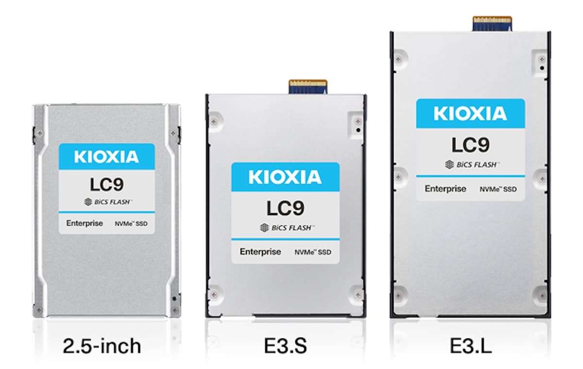
The race for AI infrastructure is often measured in GPUs, interconnections, and data centers, but increasingly it’s decided in a less glamorous area: memory and storage. In this context, Kioxia (alongside SanDisk, its industrial flash partner) appears to be gearing up for a move that, if confirmed, targets the core of the “bottleneck” in large-scale deployments: accelerating production of its most advanced 3D NAND.
According to a Nikkei report cited by Tom’s Hardware, Kioxia plans to begin manufacturing its BiCS10 generation in 2026, based on a stack of 332 layers, despite its previous plan to introduce this leap in the second half of 2027. The same information indicates a dual-strategy: BiCS10 would be produced at Fab 2 (Kitakami, Iwate Prefecture), while BiCS9 — with 218 layers — would be maintained at the established Yokkaichi complex (Mie Prefecture), targeting more “mainstream” products with better manufacturing economics.
Why does this advance matter from a business perspective?
The financial takeaway is clear: if demand for “enterprise” and high-density storage accelerates driven by AI, being first to market with more bits per wafer could mean the difference between capturing contracts (and margins) or competing solely on low prices.
The market has been signaling tensions. In an analysis published in October 2025, Tom’s Hardware reports that manufacturers and analysis firms are warning of a NAND and DRAM shortage scenario prompted by AI data center demand, after previous production cuts during the oversupply phase. In other words: the typical memory cycle is being amplified by AI and capacity limits.
Within this context, accelerating a new generation of high-density NAND can be viewed as a strategic move to “secure volume” in the high-end market (large-capacity SSDs, server storage, cloud platforms), where total cost of ownership and energy efficiency take precedence over raw unit price.
What does BiCS10 bring, and why does Kioxia refer to a “new technological baseline”?
From a technical standpoint — and this also impacts their bottom line — the leap isn’t just “more layers.” Kioxia has announced concrete advances for its 10th generation of 3D NAND flash: 332 layers with a roughly 59% increase in bit density over the 8th generation, along with a 33% faster interface speed, and improvements in performance and energy efficiency.
Architecturally, the company is pushing an approach known as CBA (CMOS directly connected to the array), which separates peripheral logic from the memory array before reconnecting them, aiming to improve performance and efficiency. Such decisions are not just engineering choices—they affect yields, manufacturing complexity, ramp-up times, and ultimately, margins.
The industrial piece: Fab 2 in Kitakami comes into play
For an advance in 2026 to be realistic, manufacturing capacity needs to support it. Kioxia has announced that the construction of its flash memory fab (Fab 2) in Kitakami has been completed, with operations expected to start in fall 2025. This aligns with the idea of reserving that newer facility for higher-spec nodes and products like BiCS10.
Simply put: if the market demands more density and gigabytes per rack, the industrial response is to invest in newer, better-equipped factories with roadmaps that prioritize “premium enterprise” over low-margin volume.
Risks and variables a financial reader should keep in mind
- Execution and yields: Moving to 332 layers is a demanding leap. If ramp-up is slower than expected, the market could remain tight, and contracts may shift to competitors.
- Demand elasticity: AI spending is strong but not unlimited; macroeconomic adjustments or a slowdown in hyperscale CAPEX could quickly shift priorities.
- Competition and supply discipline: Industry history shows that when multiple players expand capacity simultaneously, profitability can evaporate within a few quarters.
- Energy efficiency as a commercial argument: In data centers, “watts per TB” and rack density are no longer secondary metrics; if BiCS10 reduces operational costs, its value proposition remains viable even with a higher per-chip price.
Frequently Asked Questions
What does it mean for a NAND to have 332 layers, and why is it important for investors?
More layers translate to higher storage density per chip (more bits per area), which can improve wafer economics and enable larger capacity SSDs—key for data centers.
Will BiCS10 replace BiCS9 or will they coexist?
The strategy appears to support coexistence: BiCS9 (218 layers) for more general segments, and BiCS10 (332 layers) for high-density, high-value enterprise and cloud applications.
Why is AI driving such strong demand for NAND and SSDs?
Because large-scale AI deployments require not only computing power but also storing datasets, checkpoints, vectors, and large volumes of data for inference and continuous operation—boosting demand for flash and storage systems.
What role does the Kitakami factory play in this movement?
Kitakami (Fab 2) is a newer facility with recent equipment and a planned start-up in fall 2025, making it a natural candidate to produce high-demand products like BiCS10.
via: KIOXIA America, Inc.