
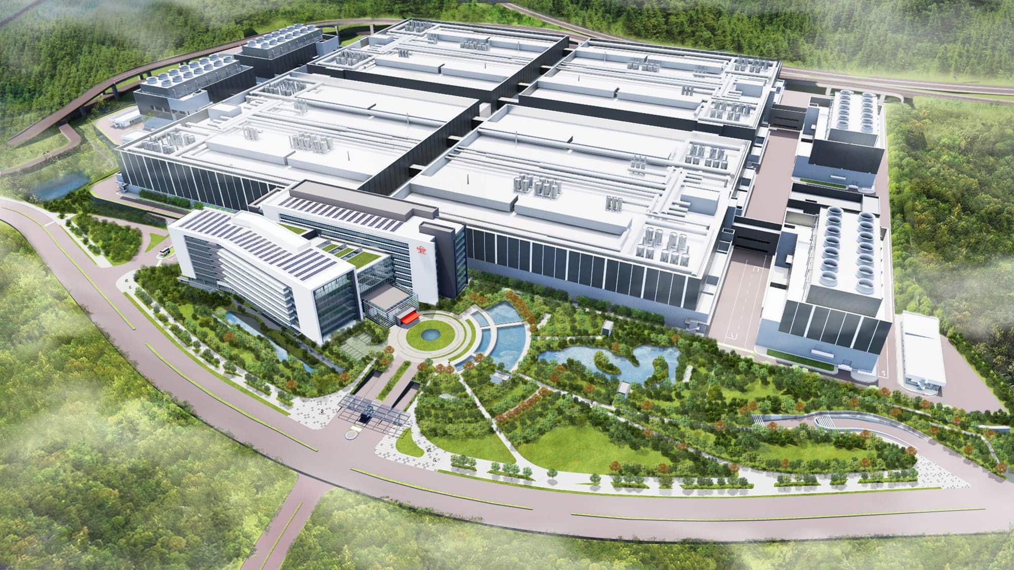
Japan’s Ministry of Economy, Trade and Industry (METI) approved a revised plan on October 16, 2026 for TSMC’s second fab in Kumamoto, which will produce 3-nanometer logic chips — the first production of this node in the country. The ministry has set a maximum subsidy of ¥645.15 billion for the plant, down from the ¥732 billion approved in 2024 for the original project. Digitimes puts that cap at around $4.1 billion. The plant belongs to JASM (Japan Advanced Semiconductor Manufacturing), TSMC’s Japanese subsidiary.
TSMC’s 3nm Kumamoto fab in 20 seconds
- Japan approves JASM’s second plant to produce 3nm logic instead of 6nm and 12nm.
- It will produce 6,000 wafers a month and start operating in December 2028.
- The maximum subsidy drops to ¥645.15 billion; the first fab’s falls to ¥409.5 billion.
The change isn’t entirely surprising. TSMC had already signaled in February its intention to bring 3nm to Kumamoto, as we reported when the second plant started preparing for that node, and Taiwan’s Investment Commission gave its approval on March 31. What was missing was certification from the Japanese government, which is what grants access to the subsidies set out under its semiconductor manufacturing support law. According to the official summary published by METI, JASM justifies the change by citing how the market has evolved following the rapid advance of artificial intelligence.
Fewer Wafers, but a Much More Advanced Node
METI’s documents make it possible to compare the two plans. The original, certified in February 2024, called for producing 12nm and 6nm logic, plus 40nm for Japanese demand, with a capacity of 48,000 300mm wafers a month, a first shipment in the fourth quarter of 2027, and an investment of around $13.9 billion ($12.2 billion without the 40nm line).
The revised plan focuses on 3nm logic with 6,000 wafers a month. The first shipment moves to the fourth quarter of 2028, operations start that December, and JASM commits to keeping production running for at least ten years. The investment covered by the subsidies is around $10.8 billion, though Dempa Shimbun reports that the project’s total investment now exceeds $15.7 billion. The exact location within Kumamoto Prefecture is still listed as pending in the document.
There’s a discrepancy worth flagging. When Taiwan approved the investment in March, several outlets cited 15,000 wafers a month. The plan now certified by Japan lists 6,000, a figure that could correspond to an initial phase, though the document doesn’t clarify this. According to Dempa Shimbun, METI has included an increase in aid in its fiscal year 2027 budget request to cover the higher cost, and makes the final support conditional on the project’s details being finalized.
The First Fab Also Changes Its Plan
The same day, METI approved a revision to the plan for JASM’s first plant in Kikuyo, which began shipments in late 2024 and had to resume operations after this summer’s magnitude-7.1 earthquake. The original plan included 22/28nm and 12/16nm nodes, with 55,000 wafers a month and an investment of around $8.6 billion. The new plan focuses on 22/28nm, plus 40nm for Japanese customers, with 45,000 wafers a month at the subsidized facilities, 50,000 across the whole plant, and an investment of around $7.3 billion. JASM attributes this to how customer demand has evolved.
The first fab’s maximum subsidy drops from ¥476 billion to ¥409.5 billion. Between the two plants, the committed public support falls from ¥1.208 trillion to ¥1.055 trillion. Local broadcaster TKU puts JASM’s total equipment investment at more than $23 billion.
JASM’s ownership structure remains unchanged: TSMC controls around 86.5%, Sony Semiconductor Solutions 6%, Denso 5.5%, and Toyota about 2%. As a condition of the subsidies, the company commits to increasing production in the event of a shortage, and TSMC commits to negotiating in good faith with the Japanese government to expand supply to the country’s customers.
Japan Wants Its Own Advanced Capacity
This will be the first 3nm production in Japan, a node TSMC has so far only manufactured in Taiwan, according to the Kumamoto Nichinichi newspaper. METI links these chips to the so-called AI transformation and to economic security, an argument it shares with its other major bet, Rapidus, which is preparing its own 2nm node and recently built a global ecosystem around that technology. The difference is that Kumamoto depends on TSMC’s technology and on the Taiwanese company keeping its priorities in Japan — something that was called into question last year when reports emerged of a pause in its projects in Japan and Germany.
Frequently Asked Questions
When will TSMC make 3nm chips in Japan?
Under the plan approved by METI, JASM’s second fab in Kumamoto will make its first shipment in the fourth quarter of 2028 and start operating that December.
How much money is the Japanese government putting in?
The maximum subsidy is ¥645.15 billion for the second fab and ¥409.5 billion for the first. Both figures are lower than what was initially approved.
What capacity will the 3nm plant have?
The certified plan lists 6,000 300mm wafers a month. In March, reports cited 15,000 — a difference the official documents don’t explain.
Who are TSMC’s partners in JASM?
Sony Semiconductor Solutions, with around 6%, Denso with 5.5%, and Toyota with 2%. TSMC holds around 86.5%.
Sources:
- METI: Certified semiconductor production facility plans
- METI: Summary of JASM’s second fab revised plan (PDF)
- METI: Summary of JASM’s first fab revised plan (PDF)
- Digitimes: TSMC’s 3nm Kumamoto plan wins Japan’s approval, qualifying for up to $4.1 billion in aid
- Dempa Shimbun Digital: METI certifies TSMC’s Kumamoto plan change
