Intel has shaken up the market with the design of Lunar Lake, a processor that blends the efficiency characteristic of ARM-based SoCs with the performance legacy of x86. New high-resolution images of the chip’s interior, published by renowned silicon photographer Fritzchen Fritz, reveal how Intel has achieved this balance in an architecture that, according to its former CEO Pat Gelsinger, could be a one-of-a-kind creation.
An Unprecedented Hybrid Approach
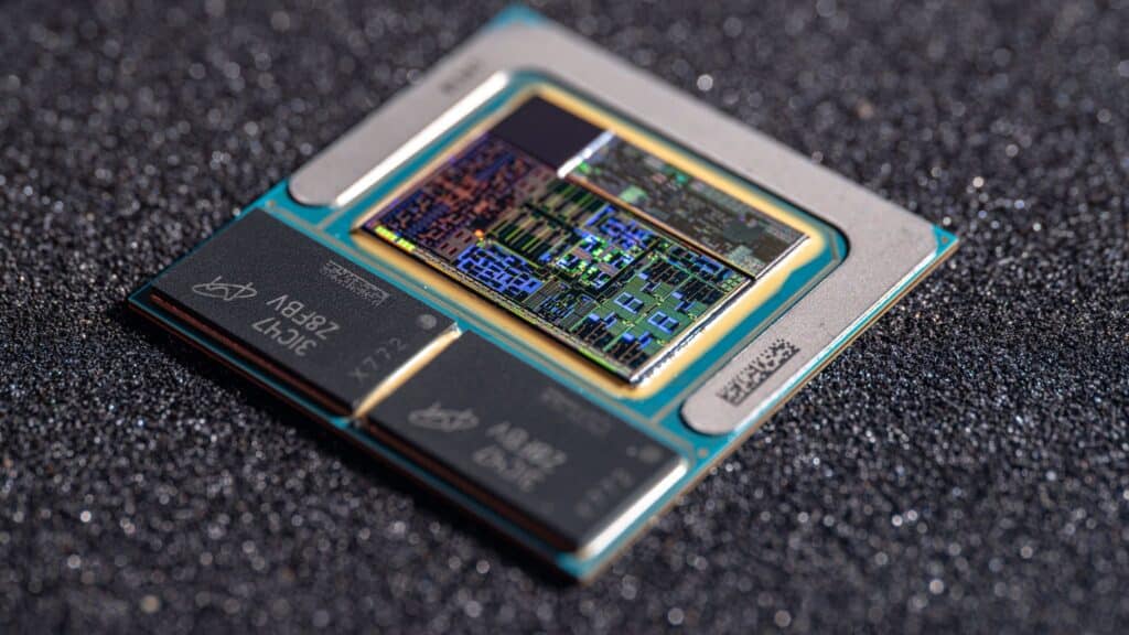
Although Lunar Lake and Arrow Lake share key technologies—such as microarchitectures and manufacturing nodes—Intel has taken completely different design paths. Lunar Lake relies on a Compute Tile manufactured by TSMC using the N3B process, housing four P cores (Lion Cove) with 12 MB of shared L3 cache and 2.5 MB of private L2 cache per core. Energy efficiency tasks fall on a cluster of E cores (Skymont), located in a "low-power island" with its own 4 MB L2 cache, isolated from the main set.
A Chip for the AI Era
Alongside the E core cluster is a Neural Processing Unit (NPU) that incorporates up to six NCE engines, with an estimated power of up to 48 TOPS (trillions of operations per second). This places Lunar Lake at the forefront of AI-accelerated computing, far surpassing previous generations of mobile processors.
Integrated Battlemage GPU and Shared Cache
The Compute Tile also integrates a GPU based on the Battlemage architecture with up to eight Xe2-LPG cores, as well as a powerful multimedia engine. All these components are unified under an 8 MB System-Level Cache (SLC), which can be shared by the CPU, GPU, NPU, and media engines. To further reduce latency, Intel has positioned the physical memory layer directly above the Compute Tile, just below the soldered LPDDR5x-8533 modules, available in 16 GB or 32 GB variants, making the memory non-expandable.
Modular Design for Drivers and Connectivity
Beneath the Compute Tile lies the Platform Controller Tile, manufactured using TSMC’s N6 process. This section contains the main input/output interfaces: USB, Thunderbolt, PCIe 4.0/5.0, as well as Wi-Fi and Bluetooth. This chiplet acts as an I/O extender, a function similar to the Arrow Lake SoC Tile, and is mounted on an active interposer based on the 22FFL process. All chiplets are interconnected thanks to advanced Intel Foveros 3D packaging technology.
Revolution or Unique Experiment?
While Lunar Lake has been designed as a strategic leap, Intel has hinted that no direct successor is planned in its leaked roadmaps. This reinforces the notion that it is a transitional architecture or a technological trial. Nevertheless, the chip offers impressive efficiency, promising graphics performance, and high integration levels, approaching the design model of Apple Silicon or Snapdragon X Elite chips.
Lunar Lake is still set to arrive in commercial laptops in 2025, but it has already generated enormous interest in the industry. With an architecture that mixes the best of both ARM and x86 worlds, its impact could be far greater than a mere experiment.
Featured Image: © Fritzchen Fritz – High-resolution view of the Lunar Lake die.
Source: Tom’s Hardware