Intel has refocused on a key area where much of the future of AI processors and data centers is being shaped: how to continue increasing computing capacity when a single “die” can no longer grow indefinitely due to physical and cost limitations. The idea isn’t new—the industry has been embracing chiplet design for years—but Intel’s message is ambitious: the size of monolithic chips is no longer primarily a lithography issue, but an advanced integration challenge.
In other words: if reticle size limits prevent manufacturing larger monolithic chips, the solution is to build “systems” within a single package by combining compute and memory modules interconnected with ultra-high-speed links, much like LEGO pieces for silicon architects. This approach doesn’t promise a specific product with fixed specs, but it clearly sets a direction to compete in the most strategic and high-cost segment of the market.
Why the reticle is less dominant than before
In lithography, the reticle defines the maximum area that can be exposed in a single pass. When a design exceeds that size, a monolithic approach becomes unfeasible or prohibitively expensive. The paradigm shift involves dividing the chip into “tiles” and recombining them in packaging, making the package the real “substrate of innovation”.
Practically, this approach enables mixing nodes (fabricating different blocks with various processes), scaling computing through modularity, and placing high-bandwidth memory (HBM) close to the silicon—crucial for AI accelerators.
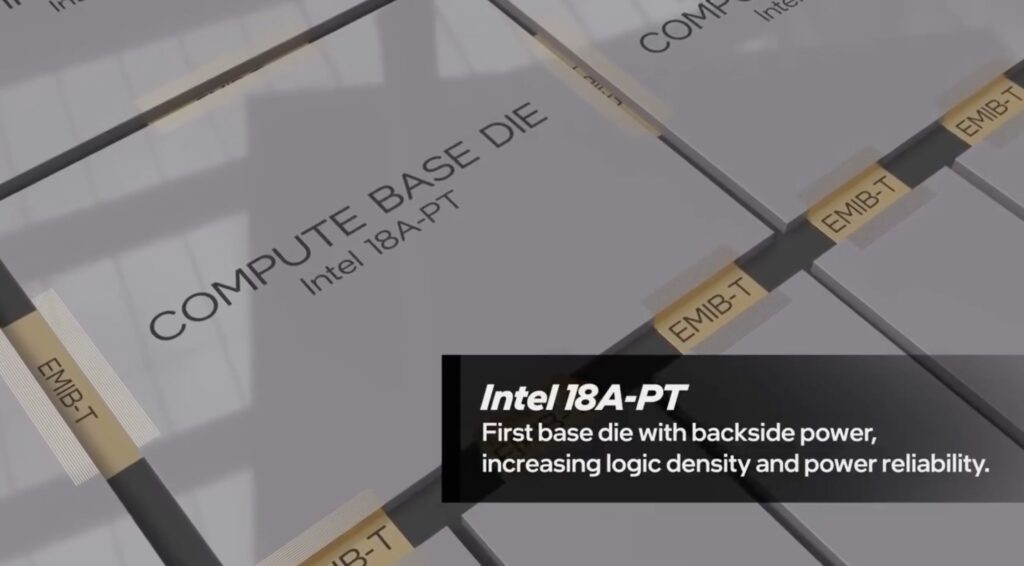
The fundamental piece: 18A-PT and “back-end” power
One of Intel’s most interesting concepts is the Compute Base Die: a base layer on which other tiles can be stacked and interconnected. As part of Intel Foundry, the company has introduced a variant of its 18A node, called 18A-PT, designed to integrate advanced packaging technologies and serve as the “foundation” of the system.
This involves a technical and economic factor: backside power delivery. Separating power and signal routes helps increase density and improve electrical behavior, which is critical when stacking blocks and increasing power consumption. Intel’s roadmap includes this technique within its process development and foundry offerings, aiming to attract clients seeking alternatives to TSMC’s leading nodes.
EMIB-T: broader bandwidth for connecting “tiles” and memory
The other pillar is interconnection. Intel has evolved EMIB (Embedded Multi-die Interconnect Bridge) to act as a “bridge” within the package, connecting chiplets without requiring a large interposer. The EMIB-T variant adds TSVs (through-silicon vias) to boost bandwidth and support larger, more complex integrations. According to Intel, this is designed, among other things, to support the transition of HBM to future generations with even greater bandwidth demands.
Simply put: if the chip is a “campus”, EMIB-T is a wider highway with more lanes and fewer bottlenecks, enabling compute and memory to communicate at the speeds required by modern AI.
Foveros Direct: 3D stacking becomes a real method, not just marketing
Meanwhile, Intel emphasizes Foveros Direct, a 3D stacking approach using hybrid bonding—direct connection with ultra-fine steps. The promise is to reduce distances, improve efficiency, and enable true stacking for multi-chip systems, with inter-layer latencies lower than in more “2.5D” approaches. Intel presents this as part of its recipe for scaling more complex packages with higher interconnection density.

The business context: AI is disrupting the market… even in packaging
This conversation isn’t happening in a vacuum. The demand for AI accelerators has made advanced packaging a critical resource: it’s not enough to manufacture good silicon; it must be encapsulated with memory and high-speed links. Reuters and other industry observers have long highlighted capacity bottlenecks in advanced packaging (and the race to expand it) as key factors influencing timelines and margins in the AI era.
Intel sees an opportunity: by positioning its integrated process + packaging + ecosystem as a complete foundry offering, it can compete in a space where wafer price isn’t everything. Differentiation will come from “the full system”: integration, supply chain, industrial capacity, and delivery times.
What’s missing: timelines, metrics, and, most importantly, real adoption
There’s a reason these presentations are filled with diagrams and light on numbers: moving advanced integration into high-volume production is difficult. In reality, viability depends on yields, defects, thermal validation, testing, assembly costs, and critically, whether customers are willing to commit to the platform.
Intel has laid out its roadmap (with 18A and future 14A as the next milestones), linking these generations to innovations like PowerVia/PowerDirect and advanced packaging techniques. But the market won’t reward promises—it will reward volume, stability, and the ability to deliver “on time and at scale”.
What the market should watch in 2026–2027
For the industry—and for anyone tracking the Intel vs. TSMC/Samsung rivalry—the “multi-chip future” will be measured by tangible signs such as:
- Foundry agreements that include advanced packaging as part of the contract;
- Demonstrations of integration with HBM and high-speed chiplet links in real designs;
- Market maturity of tools, IP, and standards (UCIe and derivatives) that reduce friction for clients;
- Industrial capacity: packaging, testing, and supply chain, not just lithography.
If Intel manages to make this approach a repeatable offering for third parties, multi-chip solutions will shift from a “design message” to a measurable competitive advantage.
Frequently Asked Questions
What does “reticle limit” mean and why does it matter?
It’s the maximum pattern size that can be exposed in lithography in a single pass. It limits the size of monolithic chips and pushes toward chiplets and advanced packaging for scaling.
Are EMIB and Foveros the same as a CoWoS-type interposer?
Not exactly. CoWoS typically uses a large interposer; EMIB employs embedded bridges to connect chiplets, while Foveros involves 3D stacking with vertical connections. These are different approaches aiming for the same goal: more bandwidth and integration.
Why is HBM so important in AI?
Because it provides massive bandwidth and low latency by being placed very close to the compute chip. In AI, moving data efficiently is just as critical as computation itself.
Will this reach PCs and consumer products, or is it solely for data centers?
The usual path is: first data centers (due to margins and demand), followed by scaled-down versions for consumers once costs decrease and packaging matures. The timeline depends on cost and industrial readiness.