Intel Foundry has once again taken a step forward in one of those areas that tend to fly under the radar compared to new CPUs or GPUs, but which could have a huge impact over the next decade: power electronics and high-frequency interconnects. The company announced that it has successfully developed, according to its own data, the world’s thinnest gallium nitride (GaN) chiplet, with a silicon base only 19 microns thick. The demo was originally presented at IEDM 2025, but Intel is now using it to reinforce a clear message: its foundry business doesn’t want to play solely in advanced logical nodes, but also in specialized materials and technologies with applications in data centers, telecommunications, and high-efficiency systems.
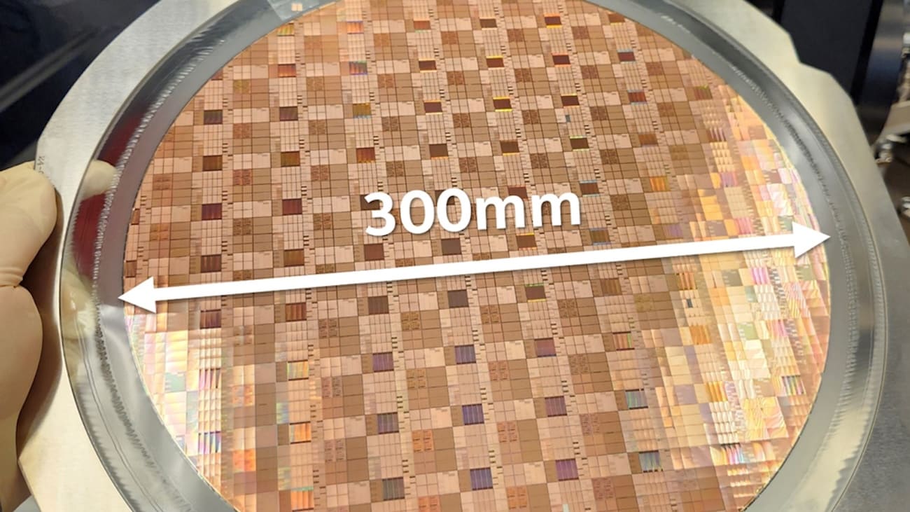
The figure alone is striking. Those 19 microns are approximately one-fifth the thickness of a human hair. But the important point isn’t just the chiplet’s thinness—it’s what Intel claims to have achieved around it: a technology based on 300 mm GaN-on-silicon wafers, with GaN transistors integrated alongside silicon-based digital circuits within the same chiplet and under a single integrated process. If this approach matures beyond the demonstration phase, Intel believes it could pave the way for smaller, faster, and more efficient components for power regulation, RF, and other high-performance applications.
More Than a Laboratory Record
The most cautious way to interpret this announcement is to separate the eye-catching headline from its actual significance. Intel talks about a technological milestone, and with the publicly available information, that seems reasonable. The company explained that this is the first complete GaN chiplet technology built on 300 mm GaN-on-silicon wafers, which is notable because this format aligns better with existing manufacturing infrastructure in the silicon industry. Additionally, the work was presented at IEDM 2025, one of the most respected technical conferences in the semiconductor device sector, lending it much more solid technical backing than a mere commercial claim.
What Intel is attempting to solve here is an increasingly visible tension in modern electronics: each new generation of systems demands more power density, higher speeds, and less space. This applies to AI accelerators, servers, telecom infrastructure, as well as various industrial and aerospace systems. Traditional silicon remains the foundation of the industry, but at certain power and frequency loads, it approaches physical and thermal limits where materials like GaN become more attractive.
Gallium nitride has long been one of the most promising candidates for this transition. Compared to silicon, GaN can operate with higher power density, switch faster, and operate more efficiently within specific thermal and electrical ranges. That’s why it is increasingly appearing in fast chargers, power electronics, RF front-ends, and advanced power systems. Now, Intel Foundry is aiming to take this potential one step further by integrating it into a chiplet format and, additionally, with monolithic digital control within the same die.
Implications for Data Centers and Networks
One of the fields where Intel sees immediate application is data centers. The company suggests that these GaN chiplets could be used in smaller, more efficient voltage regulators placed much closer to the processor. This proximity is crucial because reducing the physical distance to the load minimizes resistive losses and improves power delivery, which is especially valuable in platforms where every watt counts and where currents are increasing due to AI and accelerated computing trends.
There is also a clear message for the telecommunications sector. Intel highlights that GaN has an attractive profile for RF technology, especially for future 5G and 6G base stations, thanks to its ability to operate at very high frequencies. The company even mentions that its behavior above 200 GHz positions it well for next-generation millimeter-wave and sub-millimeter-wave bands. Additional potential uses include radar, satellite communications, or photonics, where switching speed and energy efficiency remain critical factors.
However, it’s important not to get ahead of ourselves. Intel has not announced an immediate commercial product nor a market release date for this technology. What has been shown is an R&D platform with promising reliability results, including tests such as TDDB, pBTI, HTRB, and HCI, which are fundamental for assessing whether a new device can have a practical lifespan outside the lab. This doesn’t mean production is close, but Intel aims to convey that this is more than just an academic prototype.
A Move in Line with Intel Foundry’s Strategy
This announcement also helps clarify Intel Foundry’s broader strategy. The company has been emphasizing that it wants to compete not only in advanced logical nodes but also with a diverse portfolio of differentiated technologies: packaging, materials, photonics, interconnects, and now specialized GaN chiplets. In a market increasingly demanding heterogeneous solutions, the ability to manufacture not only CPUs or GPUs but also complementary power, RF, or control components could become a significant competitive advantage.
Moreover, Intel underscores one more point: by using standard 300 mm silicon wafers, this approach could better leverage existing manufacturing infrastructure, reducing the need for radically new investments. If confirmed in industrial processes, this promise would be particularly appealing for a market seeking higher performance and efficiency without skyrocketing manufacturing costs per step.
In short, Intel isn’t just trying to sell a thin chiplet as a spectacle. It is demonstrating that alternative materials like GaN can be integrated into the chiplet domain where miniaturization, efficiency, and integration will be increasingly critical. How long this takes to become a product and its level of adoption outside research remains to be seen. But as a technological signal, this move deserves attention: in next-generation data centers and networks, the battleground won’t be limited to large processors but will also include components that deliver energy and speed more intelligently.
Frequently Asked Questions
What is a GaN chiplet and why does it matter?
It is a small chip based on gallium nitride, a material highly valued for its power efficiency and high-frequency capabilities. It matters because it can help create smaller, more efficient components for data centers, telecommunications, and advanced systems.
What exactly has Intel Foundry announced?
Intel claims to have developed the world’s thinnest GaN chiplet, with a 19-micron-thick silicon base, manufactured on 300 mm GaN-on-silicon wafers, and integrated with digital control within the same chiplet.
Is this technology ready for commercial sale?
Not yet. For now, it’s a technological demonstration presented at IEDM 2025 and now highlighted by Intel. The company cites promising results and potential real application, but it hasn’t announced a specific commercial product yet.
Where could this technology be used in the future?
Intel points to voltage regulators for data centers, 5G and 6G base stations, radar systems, satellite communications, and photonics applications, among others.