The American company is preparing for mass production of its 18A node in the second half of 2025, with Microsoft as a confirmed client and ongoing negotiations with Nvidia and Google.
Intel has launched an ambitious move in the global semiconductor market: the production of chips using its 18A manufacturing process, equivalent to 1.8 nanometers. With this advancement, it aims to position itself as a serious competitor against giants like TSMC and Samsung Electronics, targeting major clients such as Microsoft — with whom it is said to have already signed a contract — while also engaging in talks with Nvidia and Google.
According to industry sources cited by international media on May 8, Intel plans to stabilize its 18A process and enter mass production in the second half of 2025. Currently, the node is in a risk production phase. The company has also confirmed that the derived node 18A-P, which is even more efficient, has already introduced its first wafers in the factory.
During the ‘Intel Foundry Direct Connect 2025’ event, Naga Chandrasekaran, Intel’s Chief Operating Officer, stated that the 18A represents “the most advanced technology ever developed in the U.S.” and marks the gateway to a new era of advanced manufacturing. Its integration into the market would provide a competitive advantage not only technologically but also geopolitically.
Strategic Advantage: Domestic Manufacturing in the U.S.
In a context where tariffs from the Trump administration are resurfacing, Intel has a key structural advantage over its Asian competitors: it has the largest number of factories in the U.S. in the foundry sector. This local presence not only reduces the impact of tariffs but also attracts companies looking to diversify their supply chains.
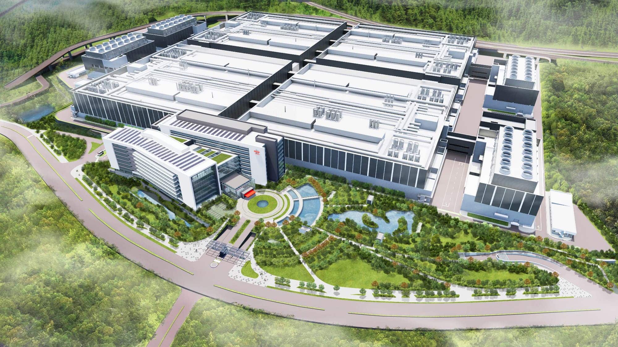
Intel has invested more than $32 billion in building two state-of-the-art factories in Arizona, an additional $4 billion in strengthening advanced packaging lines in New Mexico, and another $28 billion in Ohio, although the latter will not be operational before 2030. Work is also accelerating in Oregon and Ireland, where its Fab 34 will start producing chips with the Intel4 process this year. In Israel, Fab 38 will use EUV lithography to manufacture high-performance chips, while Malaysia will host a new advanced packaging plant.
A New Leadership for a New Strategy
The arrival of Lip-Bu Tan as CEO has been pivotal for this strategic shift. Known for his cross-functional experience in electronic design automation (EDA), packaging, and foundry, Tan brings a comprehensive vision that contrasts with the more technical profile of his predecessor, Pat Gelsinger. According to industry sources, his appointment aims to unlock major contracts and position Intel as a viable alternative to TSMC.
Global Perspective
Although Intel has historically been strong in design and manufacturing, its foundry business has been overshadowed by TSMC’s dominance in cutting-edge processes. If it secures high-volume production contracts with its 18A node, it could reshape the global semiconductor landscape.
The coming months will be crucial in determining whether Intel’s bet will pay off. If it meets its production deadlines and consolidates partnerships with strategic clients, it could regain lost leadership and once again be at the forefront of the industry.
Source: Chosun