The competition in the semiconductor industry has reached a new level with the unveiling of the latest advances in lithographic processes. During the International Solid-State Circuits Conference (ISSCC), Intel and TSMC revealed their respective innovations, solidifying their battle for technological supremacy in chip manufacturing. While Samsung remains in the background and Mediatek focuses on developing new architectures for networks, Intel has made a significant statement with its Intel 18A node, which has achieved an SRAM HD cell density of 38 Mb/mm², matching the N2 technology from TSMC. This announcement not only reinforces Intel’s position in the semiconductor race but also marks a turning point in the transition towards more efficient and scalable technologies.
The Evolution of SRAM Cells in the New Generation of Chips
To understand the significance of this milestone, it’s essential to recognize the different types of cells used in the manufacturing of processors and graphics chips:
- HP Cells (High Performance): Designed to maximize performance, though with higher energy consumption. Commonly found in high-performance CPUs, such as those used in gaming and workstation environments.
- HD Cells (High Density): Prioritize transistor density in a smaller area, optimizing energy consumption and increasing cache storage capacity. Typically found in server processors and some GPUs.
- HC Cells (High Current): Developed to handle high currents, primarily used in power management within chips.

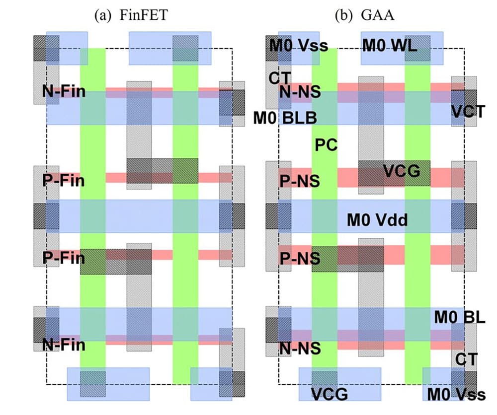
In the current transition from FinFET to Gate-All-Around (GAA) technology, the optimization of these cells is crucial for enhancing energy efficiency and processing capacity.
TSMC N2: Efficiency and Performance with SRAM HD and HC
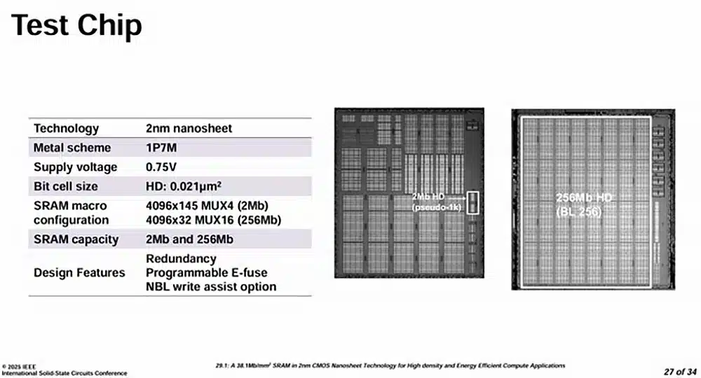
TSMC has introduced its N2 technology, achieving a density of 38 Mb/mm² in SRAM HD, representing a 12% increase over the previous generation (N3). Additionally, its HC cells have seen an 18% increase in density, thanks to its Design Technology Co-Optimization (DTCO) approach, which optimizes transistor structure and positioning within the chip.

One of the key highlights of TSMC’s advancement is the implementation of a Double-pumped system, which enhances the performance of SRAM cells in artificial intelligence (AI) and high-performance computing (HPC) tasks. Furthermore, energy efficiency has significantly improved, with an 11% reduction in consumption and a 19% increase in overall efficiency.
Intel 18A: Responding to TSMC’s Dominance
Intel has not fallen behind and has announced that its 18A node has achieved the same density of 38 Mb/mm² in SRAM HD, placing it on equal footing with TSMC in this area. Although Intel still lags in logic density, the company has chosen a more balanced design, combining performance and efficiency.
One key element in Intel’s advancement is the implementation of PowerVia, its innovative power distribution technology. Unlike TSMC, which has not incorporated a similar solution at this node, PowerVia enhances density by 10%, optimizing power supply to the transistors and reducing voltage drop.
Another significant milestone is that Intel has achieved frequencies of 5.6 GHz at 1.05V in HCC cells, demonstrating a clear performance advantage over TSMC’s solutions.
Mediatek and Synopsys: Innovation in Networking and Energy Efficiency
While Intel and TSMC dominate the conversation in high-performance chip manufacturing, other companies like Mediatek and Synopsys have made strides in specific areas.
Mediatek’s Focus on TCAM Memory
Mediatek has introduced its TCAM technology, specifically designed for use in switches and routers, two segments that require high-efficiency and low-latency memory. Its DGSL TCAM architecture promises to reduce energy consumption by up to 37.4%, representing a significant improvement for data centers and networking devices.
Synopsys Surprises with 38 Mb/mm² Density at 3 nm
Synopsys has succeeded in developing a 38 Mb/mm² HD SRAM at 3 nm technology with FinFET, representing a significant advancement in efficiency and scalability. Although its performance has not yet reached that of Intel and TSMC in terms of frequency, the ability to achieve this density at a larger node demonstrates the potential of architecture optimization technologies.
The Impact on the Industry and the Next Semiconductor Battle
The announcement of Intel 18A and its equivalence to TSMC N2 marks a turning point in the semiconductor industry. While TSMC continues to lead in chip production at advanced nodes for clients like Apple, NVIDIA, and AMD, Intel has shown it is prepared to regain ground in processor and graphics chip manufacturing.
Additionally, competition will intensify with the emergence of other players like Samsung, which is working on maturing its 3 nm processes, and companies like Google and Amazon, which are developing their own custom chips for AI and cloud computing.
On the other hand, infrastructure providers like AWS, Microsoft Azure, Google Cloud, and Stackscale (Grupo Aire) play a fundamental role in the adoption of these new technologies, as they enable companies of all sizes to access cutting-edge hardware without the need for significant upfront investments.
Conclusion: A New Era of Computing
The evolution of semiconductor technology continues at a breakneck pace, and the advancements presented by Intel, TSMC, and other key players are laying the groundwork for the next generation of devices and applications. With the arrival of more efficient and powerful chips, the impact on sectors like artificial intelligence, cloud computing, and mobile devices will be significant.
As the battle for semiconductor leadership continues, one thing is certain: the future of computing will depend on who can manufacture the most advanced and efficient chips at scale.
Source: El Chapuzas Informático

