Intel is once again making moves in its most delicate plan in recent years: turning its foundry division for third parties into a viable and, if possible, competitive business against industry leaders. The message beginning to take shape at the start of 2026 is twofold. On one hand, the Intel 18A node — which until recently was considered mainly a “for internal use” component — is starting to emerge as a real candidate for external clients. On the other hand, advanced packaging is becoming the most immediate trump card to attract large contracts before the most cutting-edge nodes reach full industrial maturity.
The takeaway is clear: if Intel wants its foundry business to reach 2027 with chances to “break the mold” and avoid remaining an eternal promise, having factories and a roadmap isn’t enough; it needs commercial traction and volume. And in semiconductors, volume rarely arrives without two ingredients: confidence in production capacity and a value proposition that doesn’t rely solely on lithography.
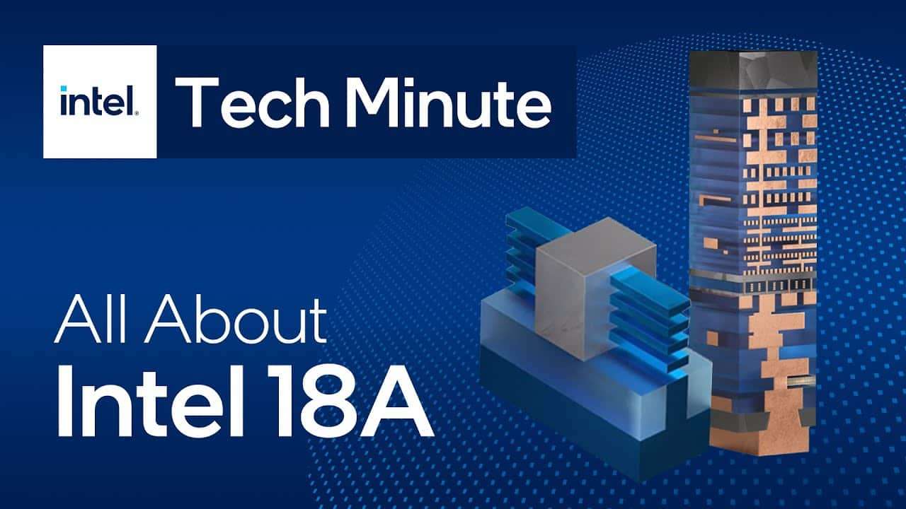
18A is no longer “just for internal use”
At the center of the discussion is Intel 18A, the manufacturing process the company presents as its significant technological leap: it incorporates RibbonFET (gate-all-around transistors) and PowerVia, its back-side power delivery architecture. On paper, this promises improvements in efficiency and density that Intel needs to compete once again at the top of performance per watt.
The key shift is that Intel is signaling that 18A could be available to external customers earlier than expected. In an industry where foundries are not “sold” with press releases but with committed production timelines and delivery schedules, this nuance matters: if the node becomes a real option for third parties, Intel gains an additional tool to attract designs… and justify investments.
Nevertheless, the keyword here is “maturity.” In advanced nodes, what’s decisive isn’t just the existence of the process but that yields, stability, and cost per wafer enable profitable manufacturing. Intel believes that 18A will become an industrial pillar, but the market will be closely watching the pace at which production normalizes.
2027: The year of breakeven (and why it matters so much)
Intel has reiterated its goal of reaching operational breakeven in its foundry business by 2027. In practice, this timeline functions as an internal deadline: the division must demonstrate that it can sustain itself with external revenue and no longer depend on the “captive” demand of the rest of the group.
The financial context explains the pressure. The company reports significant revenue from its foundry unit, but this figure includes both internal operations and work for third parties, so revenue alone doesn’t tell the whole story. The industry wants to see sustained growth in external business, with customers returning quarter after quarter and willing to pay for added value.
This is where the second pillar of the plan comes into play.
Advanced packaging: where Intel can monetize earlier
If 18A is the technological promise, advanced packaging is the business with immediate hunger. The AI era has transformed GPUs and accelerators into “systems within systems”: multiple chiplets, 2.5D and 3D interconnections, and HBM memory around the compute. This demands increasingly sophisticated integration technologies.
Intel has been pushing EMIB (2.5D bridges) and Foveros (3D stacking) for years. Recent developments include Foveros Direct 3D (a hybrid 3D bonding approach) and proposals like EMIB-T, which aim to scale interconnectivity and density for even larger packages. The industrial subtext is clear: even if a client fabricates part of the silicon outside Intel, they might still need Intel to assemble, validate, test, and turn it into a deployable final product for servers.
This gives Intel a practical advantage: packaging can generate meaningful contracts without requiring the entire chip to be fabricated on its newest nodes. In other words, it can be a nearer-term revenue stream while 18A and the next generation (such as 14A) continue to mature.
What it means for the ecosystem
For chip designers, integrators, and major computing buyers, Intel’s movement introduces an interesting variable: the possibility to diversify risks. In a market heavily dependent on a few leading foundries and with demand driven by AI, any credible alternative is closely watched — even if only for certain puzzle pieces (like packaging and testing).
However, the challenge remains monumental. Gaining trust isn’t achieved with a slide: it requires meeting deadlines, delivering quality, and maintaining controlled costs. Intel’s recent history, marked by delays in various transitions, raises the credibility bar especially high.
Summary Table: Key Pieces of Intel’s Plan
| Element | What it is | Purpose | Main Risk | Timeline |
|---|---|---|---|---|
| Intel 18A | Advanced node with RibbonFET and PowerVia | Compete in performance/efficiency and attract external clients | Yields, wafer cost, ramp-up | 2026–2027 |
| Intel 18A-P | Refined variation of 18A | Additional improvements and better fit for third parties | Same dependency on industrial maturity | 2026–2027 |
| Intel 14A | Next major node in the roadmap | Broader commercial offering in the medium term | Depends on closing customers and execution | 2027+ |
| EMIB / EMIB-T | 2.5D interconnect (and scalable evolution) | Integrate chiplets and memory in complex packages | Complexity, integration, and testing costs | Already (growing) |
| Foveros / Foveros Direct 3D | 3D stacking and hybrid bonding | Density, efficiency, and AI-style packages | Manufacturing and yield in 3D integration | Already (growing) |
A strategic shift: selling “systems” rather than just wafers
Ultimately, Intel seems to accept a fundamental market reality: modern foundries aren’t just about “printing transistors”. They offer a complete industrial stack: process + packaging + testing + supply chain + execution capacity. If Intel can turn packaging into a solid revenue stream and demonstrate that 18A can serve external clients reliably, 2027 could shift from a defensive horizon to a pivotal turning point.
But the key remains the same: customers, volume, and fulfillment. In semiconductors, second chances exist… but they’re always accompanied by a ticking clock.
Frequently Asked Questions
What is Intel 18A, and why is it so important in 2026?
It is an advanced Intel node incorporating RibbonFET and PowerVia. It matters because it’s the technical foundation for competing in performance and efficiency, and because Intel is starting to consider it as an option for external customers.
What does “advanced packaging” mean, and why might it be deployed before the node?
It involves technologies to connect chiplets and memories (2.5D/3D) in a single package. It can generate revenue earlier because a customer might want packaging and testing even if part of the silicon is fabricated elsewhere.
What is Intel Foundry’s “break-even” target for 2027?
It’s the goal to reach a neutral operating margin in the foundry division. Practically, it means the business should sustain itself without ongoing operational losses.
Why offer 18A to external customers if Intel already has 14A on the roadmap?
To generate interest and designs earlier, leverage market momentum, and avoid limiting commercial offerings to a later node. If 18A works for third parties, Intel can accelerate revenues and traction.