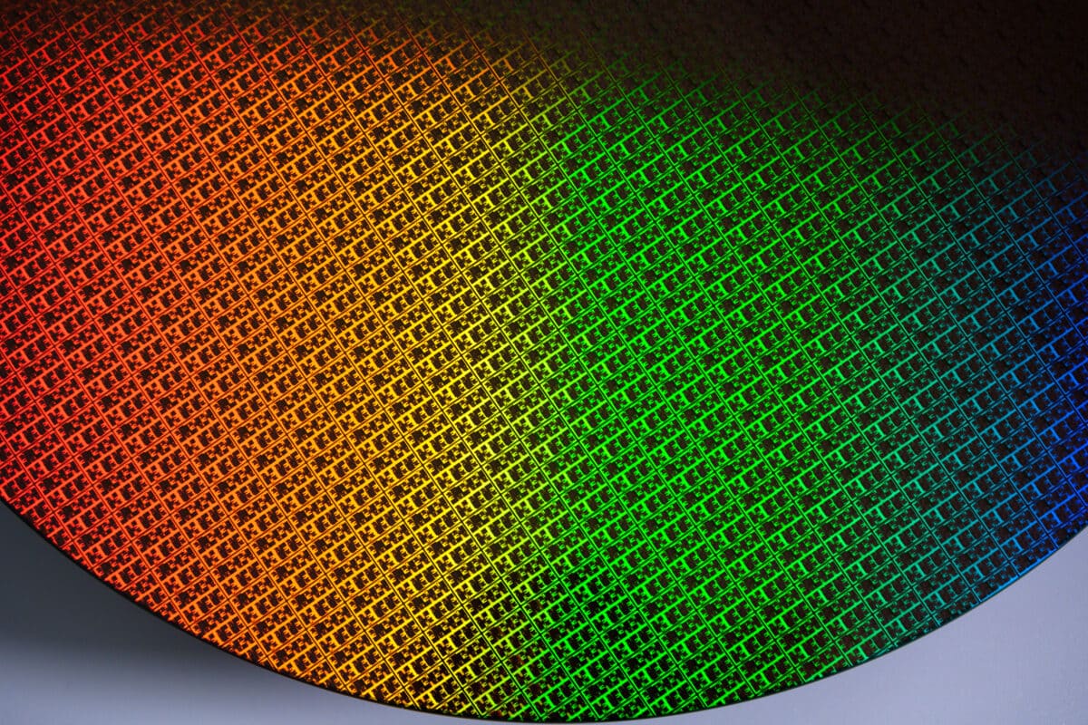
Intel Foundry delivered a very clear message to customers, partners, and investors at VLSI Symposium 2026: its Intel 18A-P node is now in risk production. This new technology is the first performance upgrade within the Intel 18A family and comes with a significant promise for the company’s chip manufacturing business: increased performance, lower power consumption, improved thermal behavior, and design rule compatibility with Intel 18A.
This news matters because Intel is not only competing as a processor designer. It is also striving to rebuild its position as an advanced foundry for third parties, a market dominated by TSMC and targeted by Samsung. In this context, every process advance counts. Intel 18A-P must demonstrate that the company can deliver competitive, reusable, and attractive nodes for external clients designing high-performance chips, especially for AI, servers, and advanced computing systems.
Risk production does not equate to volume manufacturing. It is an earlier phase designed to validate fabrication, performance, design, and industrial readiness before larger-scale deployment. Still, it marks an important milestone: Intel affirms it is on schedule with the commitments made to clients and partners last year.
Intel 18A-P: More performance without breaking compatibility
Intel 18A-P is presented as a direct evolution of Intel 18A. The claimed improvement is about 9% more performance at the same power or 18% less power at the same performance. For modern chips, this difference is significant. It’s not just about speed gains, but about giving designers more margin to balance frequency, energy, temperature, and density.
Design rule compatibility with Intel 18A is one of the most practical aspects of the announcement. It allows reusing intellectual property, methodologies, and existing design flows with less friction. For a foundry customer, this can reduce risk, adaptation time, and migration costs.
| Intel 18A-P Feature | Declared improvement or function |
|---|---|
| Performance | 9% higher at same power compared to Intel 18A |
| Power consumption | 18% less at same performance compared to Intel 18A |
| Status | Risk production |
| Design compatibility | Compatible design rules with Intel 18A |
| Transistors | RibbonFET, gate-all-around type |
| Power delivery | PowerVia, backside power delivery |
| Cell heights | 180 nm and 160 nm |
| Contacted poly pitch | 50 nm |
Intel has also detailed several technical optimizations: a new transistor option called Power Boost, improvements in thermal resistance, reduction of via resistance, tension engineering for PMOS, new options for low-power and high-performance transistors, and a fifth Vt pair between ULVT and LVT to provide more design flexibility.
In simpler terms, Intel is aiming for 18A-P to be an evolutionary rather than disruptive upgrade. This approach can be appealing to clients who wish to avoid a complete redesign but want a more efficient version of the node.
RibbonFET and PowerVia remain central bets
Intel 18A introduced two key technologies for the company: RibbonFET and PowerVia. RibbonFET is Intel’s implementation of gate-all-around transistors, featuring a structure that surrounds the transistor’s channel to improve electrical control and efficiency compared to FinFETs. PowerVia moves power delivery to the backside of the chip, better separating it from signals and reducing congestion on the front side layers.
At VLSI Symposium, Intel further supported the value of this combination with additional data. The company reports an 11% reduction in wiring area and a tenfold decrease in dynamic voltage drops compared to comparable front-end interconnect technology. This improvement could translate into up to a 6% increase in frequency or more than 15% reduction in dynamic power, based on Intel’s results.
| Technology | What it aims to solve |
| RibbonFET | Better transistor control and efficiency |
| PowerVia | Backside power delivery |
| Power Boost | More current and higher frequency with adjusted capacitance |
| Thermal improvements | Lower thermal resistance and better dissipation |
| New Vt options | More flexibility between speed and power consumption |
| Via optimization | Lower resistance in vertical interconnections |
These advancements are crucial because, in today’s advanced nodes, process improvements no longer rely solely on shrinking dimensions. Architectural changes in transistors, power delivery, interconnects, materials, and co-design now play a vital role. Intel seeks to demonstrate that its technological path can compete effectively in this new era.
Intel Foundry needs technical credibility and clients
This announcement comes at a critical time for Intel Foundry. The company has been trying for years to regain process leadership and attract external customers, but the advanced manufacturing market demands a high level of trust and reliability. Major chip designers do not choose a foundry solely based on a promising roadmap; they require performance, yield, mature tools, an EDA ecosystem, packaging, support, and dependable manufacturing capacity.
Intel 18A-P can bolster this narrative if the company demonstrates that it can bring technology to stable production. The term “risk production” is important because it allows clients to start validating designs and preparing products, but the real test will come with volume manufacturing and wafer quality.
| What Intel needs to demonstrate | Why it matters |
| Competitive yield | Defines actual cost per chip |
| Reusable design | Lower barriers for 18A customers |
| mature EDA ecosystem | Eases adoption for external designers |
| Scale production | Converts technological advances into business |
| Advanced packaging | Key for AI and HPC |
| Customer confidence | Essential to compete with TSMC and Samsung |
AI presents both an opportunity and a challenge for Intel Foundry. AI chips demand extreme performance, manage power carefully, require advanced packaging, high-bandwidth memory, and complex integration. A competitive node can open doors, but it needs to be supported by a robust ecosystem to succeed.
GaN on silicon and ruthenium: Intel looks beyond 18A-P
Intel didn’t limit itself to discussing 18A-P. The company also presented research lines pointing toward future generations of silicon technology: CFET, monolithic integration of GaN with silicon logic, and new interconnects with ruthenium.
Demonstrations included monolithic CFETs with vertically stacked NMOS and PMOS devices at a gate pitch of 45 nm, indicating a potential pathway beyond gate-all-around transistors. CFET technology is among the routes under study to continue scaling once current approaches reach their limits.
Intel also showcased monolithic integration of GaN power devices with silicon logic on 300 mm wafers, including digital control blocks of around 1,000 gates. The idea is to combine efficient power devices with digital control in a single process, relevant for energy management, power conversion, and compact systems.
| Research lines | Potential impact |
| CFET | Logical scaling beyond gate-all-around |
| GaN + silicon | Integrated power management with digital logic |
| Ruthenium subtractive | Improved interconnect scaling |
| Airgaps | Lower capacitance in metal layers |
| Backside power | Reduced congestion and better energy delivery | GAA | Higher efficiency and control of transistors |
The third area, ruthenium subtractive with airgap integration, aims to enhance interconnect scalability. Intel reports up to 35% reduction in capacitance and measurable frequency gains compared to copper. While less known to the public, this is crucial because as transistors improve, interconnects become a limiting factor in performance, power, and latency.
The real challenge lies in execution
Intel has laid out an ambitious roadmap with credible technical progress. However, the market no longer rewards process announcements alone. Industry now wants to see clients, actual chips, volumes, margins, and sustained performance.
This is especially tough because TSMC maintains a dominant position in advanced nodes and has deeply integrated itself with major clients like Apple, NVIDIA, AMD, and Qualcomm. Samsung Foundry also remains a key competitor. Intel needs to earn trust not just through technology, but through industrial discipline and reliability.
The compatibility between 18A and 18A-P might be a wise strategic move. Instead of forcing clients into abrupt changes, Intel offers a smoother evolution. If the node performs well in speed, power, and yield, it could become a preferred option for designs already considering 18A.
Why this matters for AI
AI is forcing a rethinking of silicon from multiple angles. Accelerators demand higher performance per watt. Servers need higher energy density. Data centers face thermal and power limits. Customers want chips that are more efficient so that each model generation does not cause unmanageable power consumption.
Intel 18A-P addresses this precise balance: performance, power, and thermal management. An 18% reduction in energy at the same performance can be significant when multiplied across thousands or millions of chips. A thermal improvement of 20-40%, as claimed, can help sustain higher frequencies and reduce heat dissipation issues in dense designs.
This does not guarantee that Intel will dominate external AI chips, but it indicates that its foundry aims to compete in next-generation high-performance processes. Success in combining advanced nodes, packaging, and manufacturing capacity can enable Intel to move beyond just making its own processors.
A positive sign, but not definitive
The progress of Intel 18A-P is good news for Intel Foundry’s strategy. It confirms that the 18A family continues to evolve, that PowerVia and RibbonFET are more than lab promises, and that Intel wants to showcase more technical results to the semiconductor community.
Nevertheless, the real test will come later. In semiconductors, unveiling process improvements at symposia is one thing; achieving reliable, profitable volume production for demanding customers is another. Intel must demonstrate it can meet its schedule, achieve good manufacturing performance, and offer a truly competitive alternative in a market still dominated by Asia.
The most reasonable interpretation is that Intel has taken a necessary step, not a definitive breakthrough. 18A-P reduces technological risk in its roadmap and enhances its appeal to existing 18A prospects. However, the foundry business will ultimately depend on trust, delivery, and quality of production.
Intel now has strong technical arguments to present to customers. The next step is converting those into actual orders.
Frequently Asked Questions
What is Intel 18A-P?
Intel 18A-P is the first performance enhancement within the Intel 18A family. It aims to deliver higher performance, lower power, improved thermal behavior, and design rule compatibility with Intel 18A.
What does risk production mean?
Risk production is an early phase before full volume manufacturing where chips are fabricated to validate processes, performance, and industrial readiness.
What improvements does it offer over Intel 18A?
Intel claims 9% more performance at equal power or 18% less power at the same performance, along with thermal improvements, new transistor options, and design rule compatibility.
Why is this important for Intel Foundry?
Because Intel needs to prove it can compete as an advanced foundry provider for external customers. 18A-P reinforces its roadmap and can facilitate adoption of 18A-based designs.
via: newsroom.intel