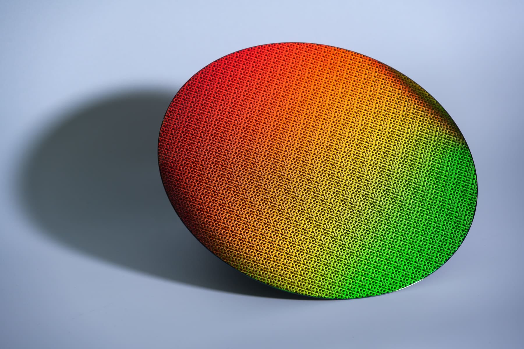
During the VLSI 2025 symposium held in Kyoto, Japan, Intel showcased the advanced capabilities of its new Intel 18A manufacturing node, which combines RibbonFET (GAA) and PowerVia technologies, achieving significant improvements in performance, energy efficiency, and density compared to previous generations like Intel 3.
A Generational Leap: Beyond Intel 3
According to the data presented in the T1-1 talk at the event, Intel 18A achieves a 30% improvement in density, a 36% reduction in energy consumption, and an increase of up to 25% in performance compared to its Intel 3 node. This advancement represents a significant evolution in Intel Foundry Services’ (IFS) strategy, consolidating its commitment to regain leadership in the semiconductor technology race.
Intel 18A includes high-performance (HP) and high-density (HD) libraries, allowing for optimized design and greater ease of implementation for its partners. The node is compatible with both Intel’s own products and third-party designs within the open foundry model promoted by Intel.
RibbonFET and PowerVia: Pillars of Innovation
The key to these improvements lies in the introduction of RibbonFET, Intel’s first gate-all-around (GAA) transistor architecture, which replaces traditional FinFETs after more than a decade of use. This architecture vertically stacks ribbon-shaped channels, allowing for better current control, greater efficiency, and scaling.
Complementing this innovation is PowerVia, a pioneering power distribution architecture located at the back of the chip (BSPDN). By moving power connections to the back, PowerVia frees up the front of the silicon for data flows, enhancing performance and reducing consumption.
The combination of these technologies enables Intel not only to achieve new levels of efficiency and power but also to simplify circuit design routing, reduce interference, and facilitate the integration of complex functions.
Comparison with Previous Generations
The presentation also contextualized these advances in relation to previous nodes. The Intel 7 process, used from Alder Lake (12th Gen) to Raptor Lake Refresh (14th Gen), started with a 10 nm base enhanced with SuperFin technology. Intel 4 and subsequently Intel 3 introduced real EUV lithography, applied in the Meteor Lake and Xeon Granite Rapids series, respectively.
With Intel 20A (~2 nm), Intel had already made significant strides towards the next generation, but now Intel 18A (~1.8 nm) surpasses it with additional advancements in scaling, performance, and efficiency. Between these two nodes, density improvements can reach up to 20%, performance can increase by up to 15%, and energy efficiency can improve by around another 15%.

Panther Lake Chips and Production in 2025
The first processors to use Intel 18A will be Panther Lake, aimed at laptops, with a planned release in the second half of 2025. Additionally, companies like NVIDIA are already evaluating this node for their future high-performance chips.
A Strategic Bet by Intel Foundry
Intel plans to offer Intel 18A as an open technology within its foundry division, allowing external companies to access this node for their own designs. With this move, Intel aims to compete more aggressively with TSMC and Samsung, providing a competitive ecosystem based on leading technologies like RibbonFET and PowerVia.
This new node not only represents a technical advancement but also a strategic assertion: Intel is determined to reclaim its position as a technological leader in semiconductor manufacturing. With high-volume production set for 2025, Intel 18A marks the beginning of a new era in chip design and manufacturing for the next generation of smart devices, data centers, and AI solutions.
Source: El Chapuzas informático