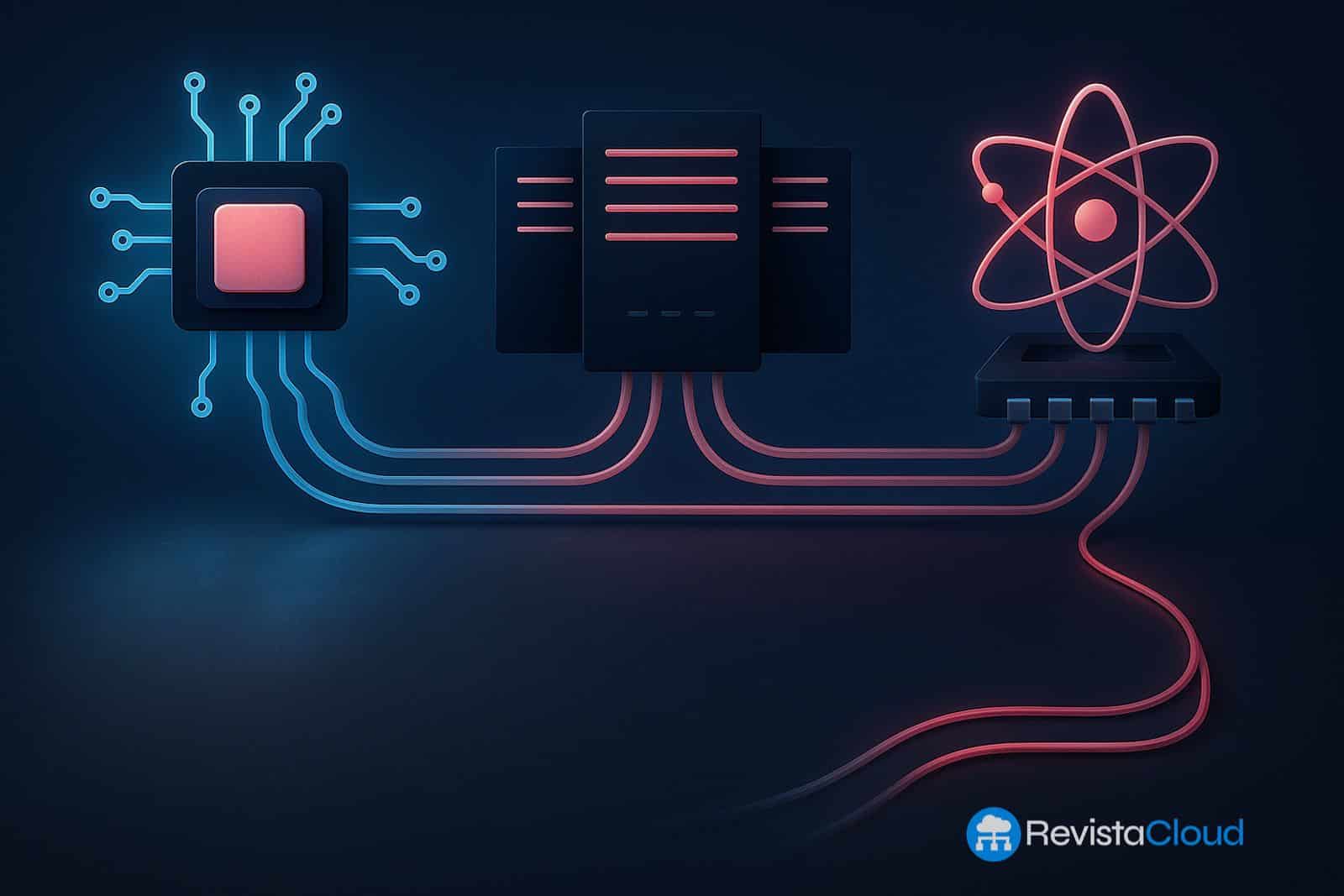
For decades, computing has advanced by moving electrons through increasingly tiny circuits. This history explains the success of microprocessors, memory, smartphones, data centers, and much of the digital economy. But the next stage won’t just involve making transistors smaller; it will also depend on how we move information in and out of the chip.
That’s where integrated photonics comes in: chips capable of guiding, modulating, detecting, and in some cases, processing light within a microscopic structure. It’s not about replacing all electronics with light, nor imagining magical computers without electrical current. The idea is more concrete and powerful: to use photons where electrons become too slow, too hot, or too energy-expensive.
Integrated photonics is already present in optical communications, data center transceivers, sensors, LiDAR, scientific instrumentation, and experimental computing platforms. Its role will grow as artificial intelligence and cloud computing drive demand for higher bandwidth, energy efficiency, and low latency.
Simply put: for years, we’ve been transmitting light worldwide through fiber optics. The next step is to bring it inside the chip.
From fiber to chip
Optical fiber made light the backbone of the Internet. A laser converts electrical signals into pulses of light, these pulses travel through kilometers of fiber, and upon reaching their destination, another component converts them back into electrical signals. This architecture has enabled the deployment of global telecommunications networks, submarine cables, large metropolitan links, and high-capacity connections.
Integrated photonics reduces that same logic to chip scale. Instead of separate optical components, it aims to integrate waveguides, modulators, splitters, filters, detectors, and other elements on a compact platform. In silicon photonics, many of these structures are manufactured using processes and techniques inherited from the semiconductor industry.
The appeal is clear: light can carry enormous amounts of data with fewer losses over certain distances, and without generating as much heat as equivalent electrical interconnections. This doesn’t mean electricity disappears; transistors remain essential for logic, memory, control, and conversion. But light can handle moving information more efficiently where electrical cabling becomes a bottleneck.
| Element | Traditional Electronics | Integrated Photonics |
|---|---|---|
| Information Carrier | Electrons | Photons |
| Main Strength | Logic calculation, memory, control | Data transport, sensors, interconnection |
| Common Issue | Heat, losses, congestion at high speeds | Light sources integration, cost, manufacturing |
| Most Mature Use | Processors, memory, digital electronics | Optical transceivers and communications |
| Next Step | Advanced packaging and greater efficiency | Optical I/O, LiDAR, sensors, photonic computing |
The most well-known limitation lies in lasers. Silicon isn’t an ideal material for efficient light emission, so industry often incorporates III-V materials, external sources, or hybrid solutions to generate optical signals. This detail explains why integrated photonics is both fascinating and challenging: it’s not enough to draw light circuits on silicon; you must create a complete system that combines optics, electronics, materials, and packaging.
Data centers: moving data now costs as much as processing it
The current driving force behind integrated photonics is data centers. AI has vastly increased the need to move data between GPUs, CPUs, memory, switches, racks, and entire clusters. Training and running advanced models depend not only on more powerful accelerators but also on those accelerators being able to exchange data without network bottlenecks.
In modern data centers, data movement can consume a significant portion of overall energy. As AI clusters grow, electrical connections inside racks and between racks begin to reach physical limits. Higher speeds mean more losses, heat, complex boards, and increased cooling costs.
That’s why companies like Intel, Nvidia, TSMC, Broadcom, Ayar Labs, GlobalFoundries, and others are closely watching optical interconnects and optical I/O. The goal is to bring optics closer to the processor—inside the chip package—to reduce electrical distances and transmit data with light as soon as possible.
For example, Intel introduces its Optical Compute Interconnect as a new class of optical connectivity capable of several terabits per second designed for next-generation computing architectures and AI infrastructure. The market trend is clear: networks are shifting from peripheral components to a central part of system design.
This could transform data center architecture. So far, much effort focused on scaling compute, memory, and Ethernet or InfiniBand networks. Integrated photonics adds another layer: optical chips capable of increasing bandwidth, reducing latency, and enhancing efficiency over high-capacity links.
It won’t solve all problems. AI will still need energy, HBM memory, advanced packaging, liquid cooling, software ecosystems, and large data centers. But integrated photonics can ease one of the most pressing issues: moving data without turning every hop into heat.
LiDAR, sensors, and light-based measurement
Light isn’t just for communication; it’s also for measurement. In LiDAR, a system emits light pulses, receives reflections, and calculates distances with high precision. This technology is used in autonomous vehicles, robotics, 3D mapping, drones, industry, defense, and advanced perception systems.
Integrated photonics can make these systems smaller, cheaper, and more robust. Instead of relying on large optical components and complex mechanisms, part of the emission, guiding, modulation, and detection can be integrated into chips. This opens the door to more compact sensors with fewer moving parts and easier mass production.
There are also applications in biosensors, chemical analysis, medical diagnostics, metrology, industrial control, and environmental monitoring. Photonic chips can detect phase shifts, wavelength changes, absorption, interference, or resonance to identify substances, measure temperature, pressure, or composition with high sensitivity.
| Application | What integrated photonics offers |
| LiDAR | More compact sensors and potentially easier to scale |
| Biosensors | Precise detection of chemical or biological changes |
| Telecommunications | Greater bandwidth in less space |
| Data centers | High-capacity optical interconnections |
| Photonic computing | Light-based operations for improved efficiency |
| Quantum technologies | Manipulation of light states on integrated circuits |
It’s important to avoid exaggerations here. Not all LiDAR systems will be photonic, nor will every optical sensor end up integrated on silicon. There are many material platforms—silicon, silicon nitride, indium phosphide, lithium niobate, silicon carbide, and hybrid combinations—each offering different advantages depending on wavelength, losses, integration, cost, or application.
What matters most is that integrated photonics allows systems that once occupied large spaces to be miniaturized onto chips. This miniaturization already transformed electronics. Now it’s beginning to do the same for optics.
Photonic computing: a real promise, but not magic
The most exciting part is photonic computing. The idea is to use light to perform certain operations, especially those involving propagation, interference, or matrix multiplication that can leverage physical properties of optical systems. For AI, signal processing, or simulation, this possibility is attractive because some tasks could be executed with lower energy consumption or greater parallelism.
However, photonic computing isn’t about replacing traditional processors entirely. Not in a general sense. Electronics remain far superior for digital logic, dense memory, precise control, and mature software ecosystems. Photonics may excel in specific operations, accelerators, and interconnects, but not necessarily in replacing entire CPUs or GPUs.
The most likely future is hybrid: electronics controlling, storing, and executing general logic; photonics handling data movement, measurement, specialized acceleration, or interconnecting computing modules. This combination could be much more powerful than a simple “light versus electrons” debate.
The history of semiconductors consistently points in that direction. No technology wins in isolation; better integration prevails. Transistors didn’t eliminate previous components—they reorganized them. Integrated photonics may do something similar: not erase electronics but add an optical layer where needed.
Why does it matter now
Integrated photonics arrives at a moment when industry faces multiple constraints simultaneously. Advanced manufacturing nodes are increasingly expensive. AI data centers consume more energy. Internal networks require more bandwidth. Sensors need to be smaller and more precise. Specialized computing seeks new ways to improve efficiency.
In this context, processing data isn’t enough; moving it efficiently is equally critical.
The good news is that integrated photonics is no longer just lab research. Silicon photonics has become a real technology in data center transceivers, and future steps include intra-package interconnects, integrated sensors, compact LiDAR, and specialized optical accelerators. Challenges remain: laser integration, large-scale manufacturing, testing, packaging, standards, and cost. But the technical direction is clear.
Europe also has an opportunity in this field. The Netherlands, Belgium, France, Germany, the UK, and Spain have research centers, industrial pilots, and companies linked to photonics. While the current focus often centers on logic chips, GPUs, and semiconductor factories, integrated photonics adds another strategic layer: technologies that will enable data movement at the scale of the next decade.
Light already connected continents via fiber optics. Now it’s beginning to enter circuits, sensors, AI racks, and computing systems. Change won’t happen overnight, but it will be profound. The chips of the future won’t be purely electronic—they’ll increasingly be a blend of electrons and photons working together.
Frequently Asked Questions
What is integrated photonics?
It’s the integration of optical components like waveguides, modulators, filters, and detectors on a chip to manipulate light at a microscopic scale.
Will integrated photonics replace electronics?
Not broadly. The most probable scenario is a hybrid architecture: electronics for logic, memory, and control; photonics for communication, sensors, and high-capacity interconnects.
Why is this relevant for AI data centers?
Because AI clusters need to move vast amounts of data between processors, memory, and networks. Optical connections can provide higher bandwidth and better energy efficiency for certain links.
What’s the connection with LiDAR?
Integrated photonics can reduce the size and complexity of LiDAR systems by integrating some of the emission, guiding, and detection directly onto chips.
What is photonic computing?
It’s the use of light to perform specific processing operations. It can be useful in specialized accelerators, AI, or signal processing but doesn’t yet replace general-purpose CPUs and GPUs.