
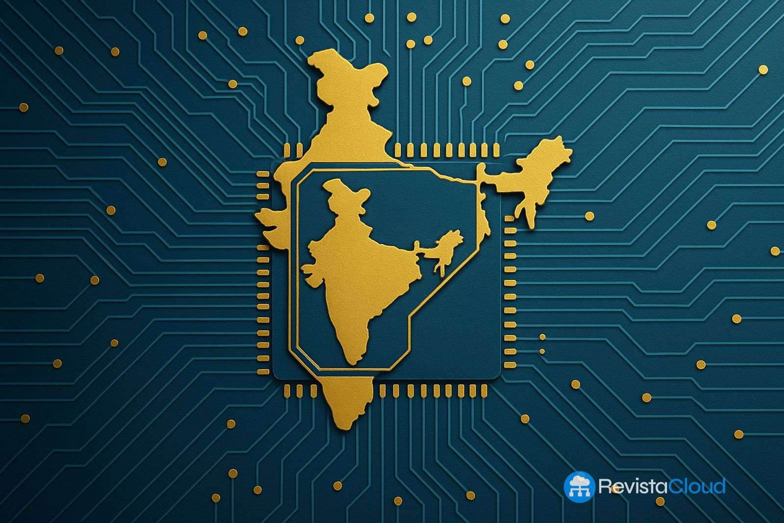
India wants to stop being just a major power in electronics manufacturing and chip design, and become one of the world’s leading semiconductor production hubs as well. To get there, the government is preparing Semicon 2.0, a new phase of its national strategy that will expand investment across nearly the entire value chain: manufacturing, design, materials, equipment, advanced packaging, research, and engineer training.
The plan starts from an important reality. India already has a huge electronics industry, but it’s still far behind countries such as Taiwan, South Korea, or the United States in advanced semiconductor manufacturing. New Delhi’s goal is to gradually close that gap over the coming years.
India Has Already Approved 12 Semiconductor Projects
The starting point was Semicon India, the program launched in 2021 and expanded with Semicon 2.0 to try to build a sustainable domestic semiconductor industry rather than simply attract a handful of isolated factories. India began with a program worth around $10 billion, aimed at backing both chip fabs and packaging facilities.
Five years later, the government says it has approved 12 semiconductor-related units, with cumulative investment of around $20 billion. Three of them reportedly began commercial production during 2026: Micron on February 28, Kaynes on March 31, and CG Power on July 4.
Semicon 2.0 is intended to now go deeper into that strategy.
Rather than focusing exclusively on building factories, India wants to develop seven major areas covering different parts of the ecosystem. These will include chip design, the equipment used to manufacture them, specialized materials, new fabs, advanced packaging, research, and workforce training.
The Big Goal: Going From 40nm to 3nm
One of the most ambitious parts of the strategy has to do with manufacturing processes.
India’s domestic ecosystem currently has 40-nanometer technology, while the world’s most advanced manufacturers are already working with considerably smaller nodes.
The government wants to design a roadmap to bring 7-to-3-nanometer technologies to India over the next eight years. Achieving that will require major investments in infrastructure, research, equipment, and highly specialized personnel.
It won’t be an easy leap. Modern fabs require extremely clean rooms, ultrapure water, highly sophisticated lithography systems, and an extensive network of specialized suppliers.
That’s precisely why Semicon 2.0 aims to go beyond simply funding factories.
India Also Wants to Manufacture Chipmaking Equipment and Materials
Another of the most interesting goals is to develop a domestic industry capable of producing some of the equipment needed to manufacture semiconductors.
Fabs currently depend on extremely specialized machinery from a small number of international manufacturers. India isn’t proposing to eliminate these imports right away, but it does want to progressively build its own capabilities so its companies can enter this part of the supply chain, a path similar to the one it’s already taking with OSAT chip packaging.
Something similar will happen with materials. According to figures cited by Indian minister Ashwini Vaishnaw, manufacturing semiconductors can require between 150 and 500 different chemicals, gases, and specialized materials. Semicon 2.0 also aims to encourage domestic suppliers for some of these components.
100,000 Engineers Specialized in Chip Design
India also has an important advantage: its experience in semiconductor engineering and design.
Major international companies already maintain sizable design teams in the country, and according to the government, Indian engineers currently take part in projects involving chips as advanced as 2nm and 3nm.
Semicon 2.0 wants to build on that foundation and raise the training target to 100,000 engineers specialized in chip design over the coming years. More than 320 universities and startups have already been given access to EDA tools through the Chips to Startup program.
India is still far from directly competing with the major advanced manufacturing powers. Still, its strategy is starting to show an important difference from previous attempts: it’s no longer just trying to build factories.
With Semicon 2.0, it wants to simultaneously develop chips, packaging, materials, equipment, research, and talent. The real challenge will be whether that enormous industrial and technological base can be transformed over the next decade into a semiconductor ecosystem capable of competing on a global scale.
Frequently Asked Questions
What is India’s Semicon 2.0 strategy?
Semicon 2.0 is the next phase of India’s national semiconductor strategy, expanding investment beyond chip fabs into design, equipment, materials, advanced packaging, research, and engineer training.
How many semiconductor projects has India approved so far?
India’s government says it has approved 12 semiconductor-related units under the original Semicon India program, with cumulative investment of around $20 billion, including three that started commercial production in 2026: Micron, Kaynes, and CG Power.
What manufacturing node is India targeting with Semicon 2.0?
India’s domestic ecosystem currently works with 40-nanometer technology. The government wants a roadmap to bring 7-to-3-nanometer technology to the country within the next eight years.
How many chip design engineers does India want to train?
Semicon 2.0 aims to train 100,000 engineers specialized in chip design, building on a base where more than 320 universities and startups already have access to EDA tools through the Chips to Startup program.
via: organiser
