On August 7, 2024, Imec, a global leader in research and innovation in nanoelectronics and digital technologies, presented significant results in the field of High NA (Numerical Aperture) Extreme Ultraviolet (EUV) lithography. These advances were achieved at the ASML-imec High NA EUV Lithography joint laboratory in Veldhoven, Netherlands.
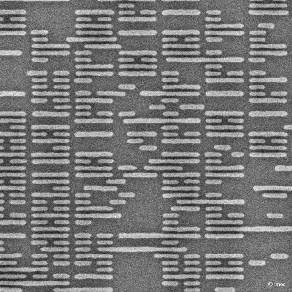
Imec’s research has successfully demonstrated logic and DRAM structures printed with a single exposure using the High NA EUV scanner (TWINSCAN EXE:5000). Achievements include logic structures with dense metal lines of 9.5 nm, equivalent to a pitch of 19 nm, and random vias with a center-to-center distance of 30 nm. Additionally, 2D features with a 22 nm pitch, and a specific design for DRAM with a 32 nm pattern, were achieved in a single exposure.
These results confirm the ecosystem’s ability to enable high-resolution High NA EUV lithography with a single exposure. Advances in lithography technology are crucial for continuing the miniaturization of logic and memory devices, enabling more complex designs and reducing costs and manufacturing process complexity.
Steven Scheer, senior vice president of technologies and computing systems at Imec, highlighted: “We are excited to demonstrate the first printing capability of logic and memory enabled by High NA in the ASML-imec joint lab, as an initial validation for industrial applications. The results show the unique potential of High NA EUV to enable the printing of aggressively scaled 2D features, improving design flexibility and reducing pattern cost and complexity.”
Luc Van den hove, president and CEO of Imec, commented: “The results confirm the resolution capability of High NA EUV lithography, aimed at sub-20 nm metal layers in a single exposure. High NA EUV will be crucial for continuing the dimensional scalability of logic and memory technologies, a key pillar for advancing roadmaps towards the ‘angstrom era’. These early demonstrations were only possible thanks to the establishment of the ASML-imec joint lab, which enables our partners to accelerate the introduction of High NA lithography in manufacturing.”
The collaboration between Imec and ASML, along with their partners, involved thorough preparatory work, including the preparation of dedicated wafer stacks, advanced resins, underlying layers, and photomasks, as well as the transfer of High NA EUV base processes to the scanner. The introduction of these advances marks a significant step towards integrating High NA EUV lithography into large-scale manufacturing, driving the future of semiconductor technology.
Source: IMEC Press Release- https://www.imec-int.com/en/press/imec-demonstrates-logic-and-dram-structures-using-high-na-euv-lithography