Imec, the well-known R&D center in nanoelectronics and digital technologies, has initiated a new pathway within its open innovation program focused on gallium nitride (GaN) technology on 300 mm wafers for low- and high-voltage power electronics. The initiative — which is part of its Industrial Affiliation Program (IIAP) for GaN — not only aims to reduce costs by moving from 200 mm to 300 mm, but also to raise the bar for what GaN can achieve in real-world applications: from point-of-load (PoL) converters for CPUs and GPUs, to onboard chargers and DC/DC converters in automotive, photovoltaic inverters, and power distribution for telecommunications and AI data centers.
This development comes with ecosystem: AIXTRON, GlobalFoundries, KLA Corporation, Synopsys, and Veeco join as initial partners in the program, clearly indicating that the move to 300 mm encompasses everything — epitaxy, processes, design, metrology, and packaging — and is not just an isolated laboratory experiment.
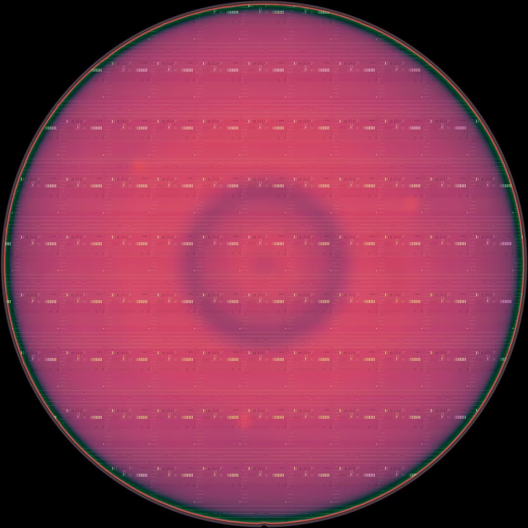
Why 300 mm matters for GaN
Over recent years, GaN has gained momentum thanks to fast chargers and more efficient, compact power supplies. Its proposition: higher power density and better conversion efficiency than traditional silicon, with direct benefits in form factor, weight, and power consumption. The industry trend has been to migrate manufacturing from 150 mm wafers to 200 mm; now, Imec takes the next step: 300 mm.
The increase in wafer diameter is not just about capacity. Opening GaN to 300 mm infrastructure — with equipment and methodologies inherited from the CMOS ecosystem — enables utilizing more advanced lithography, metrology, and process control tools. The result: more aggressively scaled devices, improved uniformity, and, in the long run, higher yields per run, which drives down unit costs.
Stefaan Decoutere, fellow and director of the GaN power program at Imec, summarizes it as follows: “The benefits of moving to 300 mm go beyond mere ‘upscaling’. Our CMOS-compatible GaN technology accesses state-of-the-art 300 mm equipment, enabling us to develop more advanced power devices.” Among his examples are the high-electron-mobility transistors (HEMTs) with aggressively scaled p-GaN gates for low-voltage applications, ideal for point-of-load converters that power CPUs and GPUs with more efficient energy distribution within the system.
What will Imec develop (and on what substrates)
The technical roadmap for this new pathway features two major phases:
- Base platform for low voltage (≈ 100 V and above).
- Architecture: lateral p-GaN HEMT.
- Substrate: silicon 300 mm (Si(111)).
- Priority process modules: p-GaN etching and ohmic contact formation.
- Goal: establish a reproducible platform for PoL and conversion stages in demanding computing environments.
- Transition to high voltage (≥ 650 V).
- Substrates: QST® (substrate engineering with polycrystalline AlN core), CMOS-compatible, and in semi-standard format for 300 mm.
- Mechanical challenges: bow control and mechanical strength of 300 mm wafers — two critical variables when transferring epitaxial GaN stacks to larger diameters.
Imec emphasizes that the launch of this 300 mm pathway comes after validating wafer handling for 300 mm substrates and completing mask development. The plan is to have full 300 mm capacity installed in the 300 mm cleanroom by the end of 2025. The roadmap is thus immediate and strategic.
From research to product-ready system: GaN moving toward commercialization
The fundamental justification is already visible in the market: smaller, cooler GaN chargers, PoL power supplies with fewer losses, and DC/DC stages and inverters with improved efficiency per liter. Imec indicates that these building blocks will be key to decarbonization and scale electrification: in automotive (onboard chargers, battery converters), photovoltaics (string inverters and microinverters), telecom (rectifiers, 48 V distribution), and the ‘electric plumbing’ for AI data centers, where every efficiency point counts.
While moving to 300 mm doesn’t automatically make GaN cheaper, it does bring it closer to a cost and scale advantage that the Si/CMOS ecosystem has already exploited for decades. More importantly, it aligns design, epitaxy, processing, and integration under a common umbrella of 300 mm equipment and methodologies, something that Imec considers crucial — a leap forward from their pioneering work with 200 mm GaN.
A complete ecosystem from day one
Imec has announced its first partners in this program as AIXTRON, GlobalFoundries, KLA Corporation, Synopsys, and Veeco. This selection covers the essential components:
- AIXTRON and Veeco: epitaxy (MOCVD reactors) and related processes for GaN growth on 300 mm wafers.
- KLA: metrology and inspection, crucial for defect control and uniformity at large diameters.
- Synopsys: design tools and device modeling to close the loop between layout, simulation, and manufacturing.
- GlobalFoundries: foundry capacity and industrial pathway to accelerate the transition to mass production once processes mature.
“The success of 300 mm development depends on a robust ecosystem that pushes forward—from epitaxial growth and process integration to packaging solutions,” notes Decoutere. Again, the key isn’t only technical; organizational factors are equally critical.
What GaN devices might emerge from 300 mm?
Although the program note doesn’t promise specific products — Imec’s role is in research and transfer — the likely device types are clear:
- Low-voltage lateral p-GaN HEMTs, with scaled gates and minimized parasitics for PoL applications in the few tens to ~100 V range. These modules, integrated into VRMs and PDNs in servers and accelerators, enable more efficient electrical distribution (e.g., 48 V chains close to the load).
- High-voltage devices (≥ 650 V) on QST® substrates — for AC/DC and DC/DC stages in EVs, photovoltaics, and telecom. Here, GaN competes on power density and efficiency against SiC and superjunction silicon.
In both cases, the industry’s key metrics are kW/liter (density), W lost per kW switched (efficiency), EMI control, and reliability (thermal and electrical robustness). Scaling critical modules to 300 mm enhances manufacturability and cost-effectiveness.
Remaining challenges
- Wafer mechanics: bowing and mechanical strength at 300 mm require optimizing epitaxial stacks and stress strategies.
- Contacts and p-GaN: precise etching and low-resistance contacts are sensitive modules for improving efficiency without compromising reliability.
- Variability and yield: statistical control (via critical dimension, thicknesses, defectivity) is key to costs.
- Packaging: encapsulation (co-packaging, advanced substrates, thermal integration) will be crucial to translate die-level advantages into the system.
Imec plans to tackle these fronts jointly with its partners, leveraging 300 mm metrology, TCAD simulation, and design flows that enable rapid iterative development from technology to application.
Timeline: 2025 as a pivotal year
The Belgian organization aims to have its full 300 mm capacity installed in its cleanroom before the end of 2025. From there, the GaN pathway will need to solidify the low-voltage platform and transition to high voltage with QST. Since wafer and mask handling validation is already complete, the focus will shift to process stabilization: module production and design window closing to enable industrial-scale adoption by the ecosystem.
Implications for the power supply supply chain
If 300 mm GaN lives up to expectations, the cost-performance equation in power supplies could tilt even more in its favor in segments where it already competes: fast chargers, server PSUs, telecom, and residential/commercial photovoltaics. In automotive, the combination of high frequency, smaller size, and higher efficiency in DC/DC stages can help streamline and simplify systems.
For telecom and AI data centers, efficient distribution — such as 48 V with local PoL — is a direct pathway to energy savings and increased density. If scaled low-voltage p-GaN HEMTs show controlled variability and cost competitiveness, their impact could become apparent in motherboards and backplanes.
Frequently Asked Questions
What advantages does 300 mm wafer GaN have over 200 mm?
Moving to 300 mm allows utilization of more advanced CMOS equipment and methods, improves process uniformity and performance, and helps drive down per-device costs. It also opens the door for more aggressively scaled GaN devices, such as low-voltage p-GaN HEMTs for point-of-load converters in CPUs and GPUs.
What substrates will Imec use for high voltage (≥ 650 V)?
Imec will use QST® substrates (CMOS-compatible with polycrystalline AlN core) in 300 mm format, designed to handle mechanical stress and ensure stability when scaling GaN stacks to larger diameters.
Which power applications will benefit first from 300 mm GaN?
Low-voltage PoL in computing (CPUs/GPUs), onboard chargers, DC/DC converters in automotive, PV inverters, and electric distribution in telecom/data centers. All share interest in efficiency, density, and size/power reduction.
Who are Imec’s first partners in the 300 mm GaN open innovation program?
AIXTRON, GlobalFoundries, KLA Corporation, Synopsys, and Veeco. They cover key sectors: epitaxy, foundry, metrology, design, and process equipment, respectively, to accelerate the platform’s maturity.
via: imec-int