Google reportedly commissioned Intel Foundry to manufacture over three million TPUs, its proprietary AI accelerators, with a delivery expected by 2028. The operation has not been publicly confirmed by either company, but if it materializes as such, it would represent one of the largest external endorsements for Intel’s foundry strategy and a clear signal of where AI infrastructure is headed: increased capacity, more suppliers, and less dependence on a single manufacturing supply chain.
This move should not be interpreted as a break with TSMC, but rather as a diversification decision. Demand for AI chips continues to grow at a rate difficult for even current leading-edge manufacturers to absorb. For Google, securing additional capacity for future generations of TPU involves protecting a core part of its business: Gemini, Google Cloud, and applications like Search, Photos, or Maps, which Google directly associates with its own accelerators.
TPUs Have Become a Strategic Piece for Google
Tensor Processing Units (TPUs) are ASICs designed by Google to accelerate machine learning workloads. The company has been using them for years in foundational models, inference, training, recommendation, code generation, vision, voice, and personalization. Google Cloud presents them as optimized accelerators for agents, large language models, and AI applications at scale.
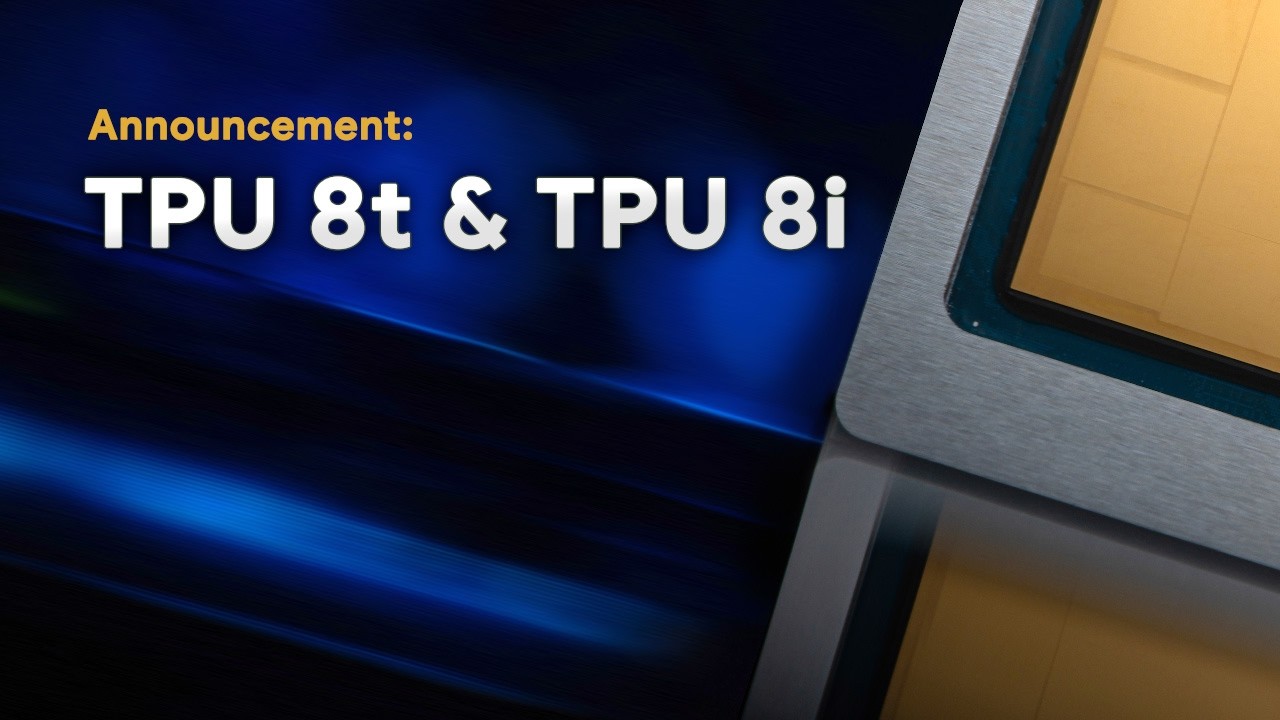
The latest officially announced generation, TPU 8t and TPU 8i, reveals the scale of the challenge. TPU 8t is geared towards training large models, while TPU 8i focuses on low-latency inference for agent-based workloads. Google claims TPU 8t allows superpods of 9,600 chips, two petabytes of shared HBM memory, and 121 ExaFLOPS of compute, while TPU 8i incorporates 288 GB of high-bandwidth memory, 384 MB of on-chip SRAM, and a 19.2 Tb/s ICI interconnect.
| Element | What it means for Google |
|---|---|
| Proprietary TPUs | Less direct dependence on third-party GPUs |
| TPU 8t | Training large models and developing foundational models |
| TPU 8i | Low-latency inference for agents and production services |
| Google AI Hypercomputer | Integrated hardware stack including hardware, networking, storage, software, and orchestration |
| Intel Foundry as potential manufacturer | Additional capacity and supply diversification |
| TSMC | Continues to be a key player in advanced manufacturing |
| Expected delivery in 2028 | Linked to future AI infrastructure generations |
The distinction between TPU 8t and TPU 8i is also significant. Google is designing specialized chips because training models at scale and deploying inference are no longer the same problem. Training requires throughput, shared memory, and massive interconnects. Agent-based inference requires low latency, high memory bandwidth, and efficiency per dollar. In the era of agents that reason, plan, execute, and continuously learn, even small inefficiencies multiply when dealing with millions of requests.
Why Intel Needs a Client Like Google
For Intel Foundry, such an order would carry value beyond just revenue. The company has been trying for years to convince the market that it can compete as an advanced foundry for external customers, not just as a manufacturer of its own processors. This transition demands technology, industrial capacity, a design ecosystem, advanced packaging, and crucially, reference customers.
Intel’s 18A node is central to this narrative. It is presented as a 2 nm class node developed and produced in North America, featuring RibbonFET transistors (gate-all-around implementation) and PowerVia back-side power delivery. Intel states that 18A targets applications like HPC, AI, mobile processors, baseband, imaging, and defense.
The Intel 18A-PT variant is especially interesting for complex AI accelerators. Intel describes it as tailored for AI and HPC customers developing 3DIC designs, TSV, die-to-die TSV, and hybrid bonding. In documentation, Intel notes that 18A-PT enables advanced integration for high-performance workloads and multi-die designs.
Packaging also plays a role. Intel Foundry highlights that 18A-PT can connect to superimposed dies via Foveros Direct 3D with hybrid interconnects less than 5 micrometers. This capability is important because AI accelerators are no longer just “chips”: they are systems composed of chiplets, high-bandwidth memory, interposers, internal networks, and increasingly dense integration technologies.
Diversification Is Not Abandoning TSMC
The potential order from Google aligns with a supply resilience strategy. TSMC remains the dominant leader in advanced manufacturing and continues to be key for companies like NVIDIA, Apple, AMD, Qualcomm, and many others. However, concentration of demand at TSMC has become an operational and geopolitical risk for major capacity purchasers.
AI has strained every link in the supply chain: advanced wafers, HBM, CoWoS packaging, interconnection, substrates, power, data centers, and integration capabilities. In this scenario, a second manufacturer does not necessarily replace the first; it complements it. For Alphabet, having a portion of future production at Intel could provide more margin in case of bottlenecks, delays, or shifts in industrial priorities.
This logic mirrors other segments in the semiconductor supply chain. chip designers want more foundry options, regional capacity, and advanced packaging alternatives—not because TSMC is unreliable, but because the scale of AI demands redundancy and diversified supply sources.
For Intel, Google would be a particularly valuable customer because TPUs represent a real high-scale workload. This isn’t an experimental chip but accelerators powering global AI services. An order of millions would demonstrate that Intel Foundry can aspire to produce critical silicon for one of the world’s largest infrastructure operators.
NVIDIA Also Looks at Advanced Packaging
The news about Google is accompanied by another relevant detail: NVIDIA is also evaluating whether Intel’s technology could be used to manufacture a processor that combines four GPUs into a single unit. There’s no confirmed order or official confirmation yet, but the technical direction aligns with market trends.
AI accelerators are moving toward multi-die architectures. Interconnect density, chiplet latency, power delivery, cooling, and memory integration are as significant as the node itself. Intel aims to position itself there—not just as a transistor foundry but as a provider of advanced manufacturing and packaging systems.
This could be a decisive factor. The AI race is not won solely based on the smallest node but on the ability to assemble complete systems with good performance per watt, scalability, and sufficient production capacity. Google exemplifies this with its holistic approach: TPU, Axion as a host CPU, networking, liquid cooling, storage, frameworks like JAX or PyTorch, and bare-metal access are part of one integrated stack.
A comparison with NVIDIA is inevitable, but not exact. Google designs TPUs for its own cloud and services, though they are also offered to Google Cloud clients. NVIDIA sells a broader, more cross-market platform. Intel, meanwhile, seeks to become a manufacturing partner for both—those designing their own chips and those requiring advanced packaging for increasingly complex AI systems.
A Potential Turning Point for Intel Foundry
Intel needs to prove that its foundry ambitions can attract large external clients. The investment in factories, advanced nodes, and packaging is immense, and the market demands tangible results—a mix of tape-outs, production, performance, yields, and volume.
A deal with Google to produce TPUs would be a strong validation. It would also send a message to other chip designers: Intel Foundry can be a viable option to diversify production in North America, especially for AI and HPC designs. This message is timely as the US and Europe seek to bolster their semiconductor capabilities for economic, technological, and strategic reasons.
Nevertheless, caution is advised. Manufacturing over three million AI accelerators is not just about reserving capacity. It requires mature nodes, reliable yield, packaging, memory supply, validation, software, logistics, and coordination with data centers. Until Google or Intel confirm details, this order should be considered unofficial—though it aligns with current technological and industrial trends.
What is clear is the broader context: Google needs more TPUs for the agentic era, Intel needs large external customers, and the industry as a whole requires more advanced manufacturing capacity, beyond traditional bottlenecks. If these needs align, Intel Foundry might find in Google’s TPU order an opportunity it has been seeking for years.

Frequently Asked Questions
What are Google’s TPUs?
TPUs are custom accelerators designed by Google for AI workloads such as training, inference, agents, code generation, vision, voice, recommendation, and personalization.
What is the difference between TPU 8t and TPU 8i?
TPU 8t is aimed at training large-scale models, while TPU 8i is designed for low-latency inference and production agent workloads.
Why would Google turn to Intel Foundry?
To diversify manufacturing capacity, reduce reliance on a single supply chain, and secure additional production for future TPU generations.
What does Intel 18A bring to this market?
Intel 18A features RibbonFET and PowerVia, and the 18A-PT variant targets AI and HPC designs with TSV, hybrid bonding, and advanced 3DIC packaging.