
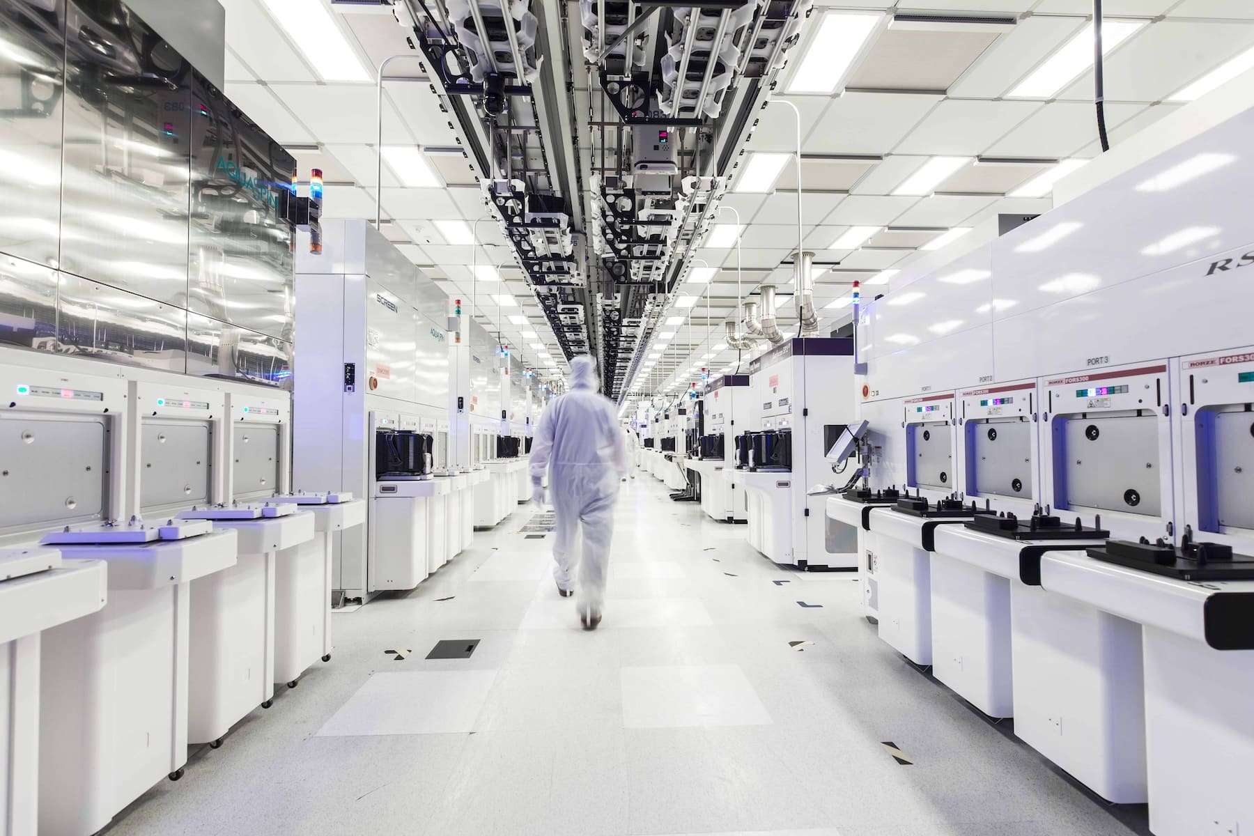
GlobalFoundries (GF) is preparing to accelerate its global manufacturing capacity as demand grows for radio frequency (RF) chips and other semiconductors tied to the rise of artificial intelligence. The company points to Singapore as one of the key pieces of this expansion, while its US fabs continue to run at high utilization levels.
GlobalFoundries’ expansion in 20 seconds
- GF is preparing more global capacity for RF chips and other technologies tied to AI.
- Singapore will play a significant role alongside the optimization of its current production lines.
- The company has not yet detailed how much it will invest or how much capacity it will add.
- GF is expanding technologies such as RF-SOI, SiGe, silicon photonics, and GaN.
- MIPS, its IP subsidiary, expects to grow its R&D team in Taiwan to 100 engineers.
The announcement comes as demand for AI semiconductors extends well beyond GPUs and other compute processors. AI infrastructure also requires radio frequency circuits, power management, connectivity, photonics, and other specialized components. GlobalFoundries is trying to grow its capacity precisely in several of those areas.
Vincent Feng, GlobalFoundries’ head for Asia-Pacific, said at a conference held in Hsinchu that the company is preparing a significant capacity expansion. However, he avoided giving specific figures, timelines, or investment amounts. According to his remarks reported by Taipei Times, GF’s fabs in the United States currently show high utilization.
Singapore gains weight in GF’s manufacturing network
Singapore stands out as one of the hubs the company wants to use to meet this demand. GlobalFoundries’ plant in Woodlands combines 300mm and 200mm manufacturing and produces specialized technologies for automotive, mobile devices, industrial, photonics, and connectivity applications.
The complex currently employs roughly 3,800 people and has 87,000 square meters of cleanroom space. GlobalFoundries puts its total capacity at the equivalent of 1.5 million 300mm wafers per year. Technologies manufactured there include CMOS, Power BCD, RF-SOI, silicon-germanium (SiGe), and silicon photonics.
The company is already making concrete moves in Singapore. In September it announced a manufacturing agreement with Monolithic Power Systems (MPS) to bring its proprietary power management technology to the advanced 300mm fab. Volume production is planned for 2027. The resulting chips are aimed at data centers, automotive, consumer electronics, and industrial applications.
SLATE technology, a wafer-bonding system designed to integrate three-dimensional structures for RF applications, is also progressing. GlobalFoundries has said that SLATE on its 9SW RF-SOI platform is ready for production and that volume manufacturing is planned for the second half of 2027. The design can shrink die size by up to 45% in certain RF structures.
The Asian plant also plays a growing role in photonics. GlobalFoundries acquired Singapore-based Advanced Micro Foundry (AMF) in 2025 to expand its silicon photonics capabilities. The company now describes its global operation as the largest specialty silicon photonics manufacturing platform among independent foundries.
AI’s rise is also driving up RF demand
The link between artificial intelligence and radio frequency may be less obvious than the one between AI and GPUs, but GlobalFoundries is betting on it. The company believes growth in data centers, wireless networks, and connected systems is creating new demand for specialized chips.
Its RF portfolio includes RF-SOI, SiGe, and RF GaN technologies, used in applications ranging from smartphones and wireless networks to satellite communications, radar, and data center connectivity.
In June 2026, GF said it was developing RF GaN, based on gallium nitride on silicon, for communications, defense, satellite, and data center applications. The company notes that this approach makes it possible to manufacture GaN on 200mm silicon wafers, combining the material’s properties with manufacturing processes geared toward higher volumes.
The company has also strengthened its GaN technology through an agreement with TSMC. In November 2025, GlobalFoundries announced it had obtained a license for 650V and 80V GaN technologies from TSMC. The stated goal was to accelerate a new generation of GaN products for data centers, industrial, and automotive applications, manufactured in the US at its Burlington, Vermont plant.
That agreement does not mean all GaN production will be concentrated in Singapore. GF keeps its RF GaN manufacturing in the United States, while Singapore takes part in other RF and specialized technologies within a distributed production network.
More activity in Taiwan and new engineers for MIPS
The strategy announced in Hsinchu also has a commercial and engineering dimension in Taiwan. Feng said GF wants to increase its local presence after years of keeping a relatively low profile in the Taiwanese market.
Geographic proximity to Singapore and Taiwan’s weight in chip design are two of the factors the company is using to strengthen its customer relationships. Ed Kaste, GlobalFoundries’ senior vice president of CMOS, said major US cloud providers are increasing their demand, and that growth is driving the need for manufacturing within the United States.
MIPS activity will also grow. GlobalFoundries’ IP subsidiary currently has 35 R&D engineers in Taiwan and plans to add more than 30 more. The longer-term goal is to reach 100 professionals, a figure comparable to its R&D teams in other regions.
The expansion reflects a strategy that goes beyond simply building new fabs. GlobalFoundries is combining added capacity, the retooling of existing lines, and the development of specialized processes to meet different types of demand — much as it has done elsewhere through manufacturing partnerships, such as its alliance with Renesas to expand chip production and secure the supply chain.
For now, though, the details needed to quantify the scope of the new global expansion are still missing. GF has not disclosed the total investment, the number of additional wafers, or a full timeline for the expansions Feng mentioned. What is confirmed is the intent to accelerate capacity and the role Singapore will play in that strategy, together with the investments and agreements already underway across its various plants.
Frequently asked questions
Why is GlobalFoundries expanding its capacity?
The company attributes the capacity increase to growing demand for RF chips and other technologies linked to the expansion of artificial intelligence, data centers, and connectivity. It also points to high utilization at some of its US fabs.
What role will Singapore play for GlobalFoundries?
Singapore is one of GF’s main manufacturing hubs and produces technologies such as RF-SOI, SiGe, silicon photonics, and CMOS. The company plans to use its facilities there as part of its global capacity expansion.
What GaN technologies does GlobalFoundries manufacture?
GF develops gallium nitride technologies for radio frequency and power management applications. In 2025 it also obtained a license from TSMC for 650V and 80V GaN technologies aimed at data centers, industrial, and automotive uses.
How many engineers will MIPS have in Taiwan?
MIPS currently has 35 R&D engineers in Taiwan and plans to add more than 30 more. Its longer-term goal is to reach 100 professionals in the country.
