Here’s the translated text in American English:
EV Group (EVG), a leader in innovative process solutions for cutting-edge semiconductor designs, is showcasing its IR LayerRelease temporary bonding and debonding (TB/DB) technology at the SEMICON Korea 2025 exhibition, taking place from February 19 to 21 in Seoul, South Korea.
Innovation in Advanced Chip and Memory Integration
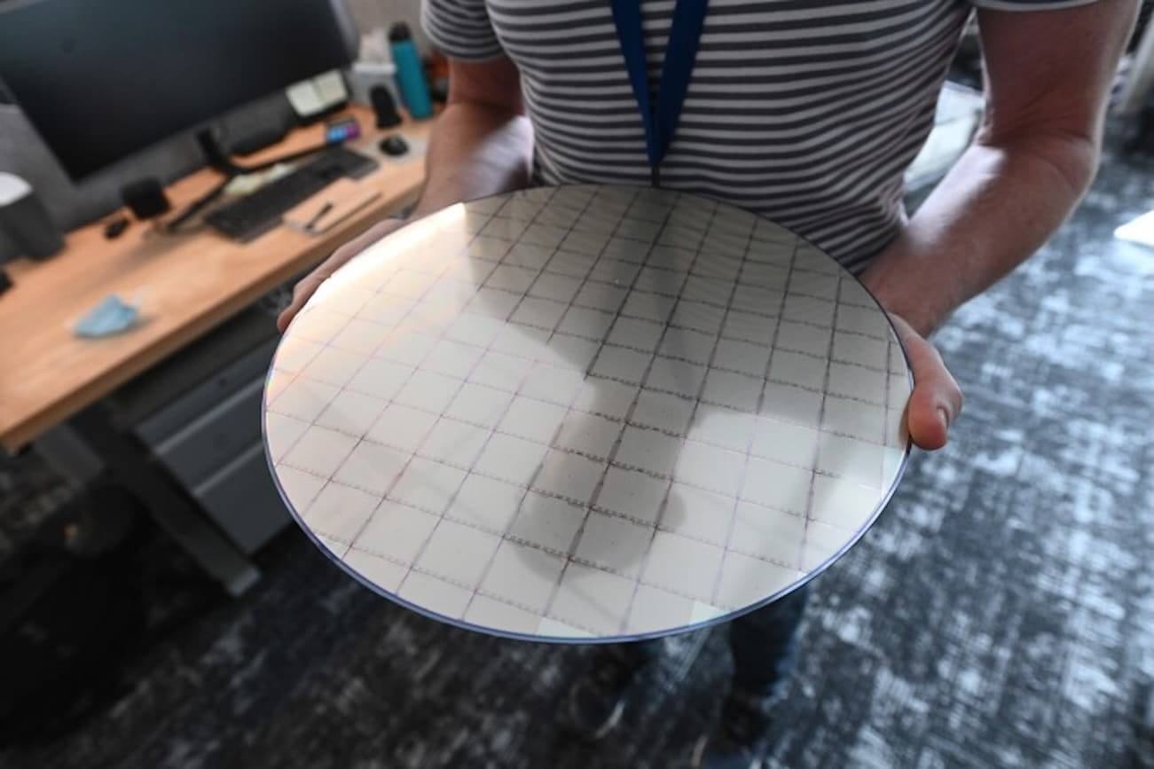
EVG, recognized for its leadership in wafer bonding technology, is presenting its IR LayerRelease solution, a laser-based infrared debonding technology designed to enhance the production of High Bandwidth Memory (HBM) and 3D stacked DRAM. These technologies are essential for applications in artificial intelligence (AI) and high-performance computing (HPC).
According to Dr. Thorsten Matthias, Regional Sales Director for Asia/Pacific at EVG: “Accelerating the development and volume production of HBM and 3D stacked DRAM is a priority for the Korean semiconductor industry. Our IR LayerRelease technology is revolutionizing the market by enabling thinner chip stacking through laser debonding, eliminating the need for mechanical debonding.”
Temporary Bonding and Debonding for Advanced Memory
HBM and 3D DRAM technologies have emerged as key solutions for AI training due to their ability to provide high bandwidth, low latency, and energy efficiency in a compact format. Temporary wafer bonding and debonding is a critical process in the manufacturing of these advanced memory types.
Traditional mechanical debonding solutions cannot provide the precision necessary for ultra-thin wafers with complex geometries. In this context, EVG’s IR LayerRelease offers significant advantages:
- Higher precision and performance
- Lower operational cost
- Reduced environmental impact
- Compatibility with future generations of memory
Technical Details of IR LayerRelease
The IR LayerRelease technology uses an infrared (IR) laser that penetrates silicon, allowing for the precise release of ultra-thin layers without damaging the carrier wafer. Unlike traditional processes, IR LayerRelease does not require glass substrates, enabling new process flows for 3D-IC and 3D sequential integration. Additionally, this technology uses inorganic solvents for post-cleaning, minimizing the ecological footprint in semiconductor manufacturing.
IR LayerRelease is integrated into the EVG®880 platform, a high-volume automated production solution.
EVG at SEMICON Korea
Attendees at SEMICON Korea 2025 interested in learning more about EVG’s solutions for AI, HPC, advanced packaging, and sustainable semiconductor manufacturing can visit booth C740 (3rd floor, Hall C) from February 19 to 21 at COEX in Seoul, South Korea.
Source: Semiconductor Digest