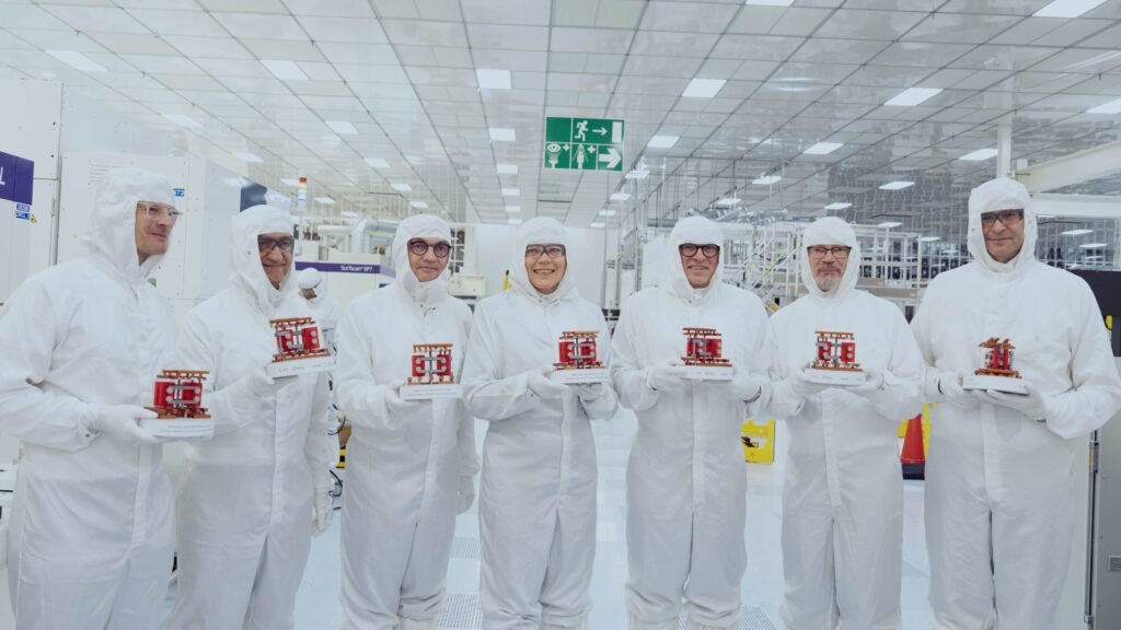
Europe aims to be part of the global conversation on cutting-edge silicon, and to achieve this, it is betting on a very specific approach: bringing top-tier research to an almost industrial scale, where ideas are tested using real tools and with real partners. This is the role of NanoIC, the largest pilot line of the European Chips Act, inaugurated in Leuven (Belgium) at the imec headquarters, with an expansion of 2,000 m² of cleanroom space that reinforces a reference infrastructure to push technology beyond the 2 nm node.
The inauguration event brought together political and industry leaders who rarely appear together at purely technical announcements: European Executive Vice President Henna Virkkunen, Belgian Prime Minister Bart De Wever, Flanders’ Minister-President Matthias Diependaele, and ASML CEO Christophe Fouquet, among other representatives of the European semiconductor ecosystem. The message was unequivocal: chips have become a strategic issue, and Artificial Intelligence is accelerating that urgency.
A “near-factory” laboratory for sub-2 nm leap
NanoIC is presented as a pilot line designed to reduce the gap between laboratory and production: an intermediate point where companies, start-ups, universities, technological centers, and manufacturers can validate processes, materials, and designs with a realism level far superior to traditional academic environments. This is a key difference in the AI era: it’s not enough to demonstrate progress; it must be industrialized without turning into a decade-long project.
Imec emphasizes that the Leuven expansion is part of a broader deployment that extends beyond a single cleanroom. Over the coming years, NanoIC will integrate more than one hundred new tools spread across imec and various European partners: CEA-Leti (France), Fraunhofer (Germany), VTT (Finland), CSSNT-UPB (Romania), and Tyndall National Institute (Ireland). Simultaneously, preparations are underway for a new expansion: the construction of an additional 4,000 m² cleanroom on the Leuven campus.
High NA EUV: the tool setting the pace
If there is a symbol of the technological “leap,” it is the High NA EUV lithography equipment from ASML. imec has confirmed that the next-generation system is expected to arrive by mid-March, and it will be one of the core components of the “best-in-class” equipment being deployed in the pilot line.
The European Commission, in its own NanoIC announcement, highlights it as a milestone: a European facility incorporating the most advanced EUV machine, focused on designing and manufacturing chips with technologies below—or beyond—2 nm. In the sector, this capability is not just seen as “more density,” but as the potential to explore new process combinations, integration, and design options that define the next generation of systems-on-chip for AI-intensive workloads.
The less visible value: PDKs to prevent blind design
Behind the sub-2 nm headline lies a practical problem: no chip ecosystem progresses if designs lack tools to work with technologies still “in the making.” Here, PDKs (Process Design Kits) come into play—kits that enable designers and engineering teams to prototype and validate decisions before mass production.
NanoIC is publishing PDKs aimed at “pathfinding,” that is, exploring future technological routes. In February 2026, the project announced an A14 logic PDK and an eDRAM memory PDK, with the goal of accelerating design in advanced logic nodes and improving options for integrable memory on chips. In earlier announcements, NanoIC also introduced an N2 pathfinding PDK incorporating advanced SRAM macros—an important piece to prevent the design of complex systems from waiting for the process to fully mature.
In other words: Europe doesn’t just want to “own machines”; it wants a community capable of designing, testing, and failing fast within a shared infrastructure.
Funding and ecosystem: a bold numbers-driven bet
The European Commission estimates NanoIC’s total investment at around 2.5 billion euros, with 700 million euros funding from the EU and another 700 million euros from national and regional governments; the remainder comes from industrial partners, including ASML. The declared goal is to accelerate critical technologies for AI, automotive, healthcare, or 6G, and to strengthen Europe’s innovation and advanced manufacturing capacity.
This approach aligns with the Chips Act’s philosophy: not just competing on volume, but on technological capacity, access to cutting-edge equipment, and a value chain less dependent on external sources when the market becomes tense.
Beyond the chip: talent and technological sovereignty
The sub-2 nm battle isn’t won solely with capital and machinery; it’s won with people. Imec emphasizes that NanoIC also aims to serve as an infrastructure for training the next generation of specialists: courses, programs, bootcamps, and initiatives with European competence centers to expand the pool of engineers and profiles capable of working on materials, processes, and SoC design.
In a market where demand for advanced semiconductors is driven by AI and supply chains remain under pressure, this pilot line sends a strategic message: Europe does not want to be just a consumer of critical technologies but also a producer of knowledge and industrial capacity.
Frequently Asked Questions
What exactly is a “pilot line” like NanoIC, and how does it differ from a chip factory?
A pilot line is an environment that allows testing processes and designs with industrial tools, but without the primary goal of volume production. It’s used to validate technology, reduce risks, and accelerate the leap to commercial manufacturing.
Why is “sub-2 nm” so relevant for Artificial Intelligence?
AI workloads demand greater energy efficiency and higher computational density. Progressing in logic nodes and system integration helps improve performance per watt and enables more complex designs within thermal and power limits.
What role does High NA EUV lithography play in this race?
High NA EUV is a key evolution of EUV lithography that allows for finer structures with better control—essential for continuing to scale and explore new fabrication techniques at advanced nodes.
What are PDKs, and why are they important in a project like NanoIC?
PDKs are “kits” connecting manufacturing and design: models, rules, and libraries that allow teams to design chips based on a specific process. Without PDKs, design progresses blindly, and development cycles slow down.
via: IMEC