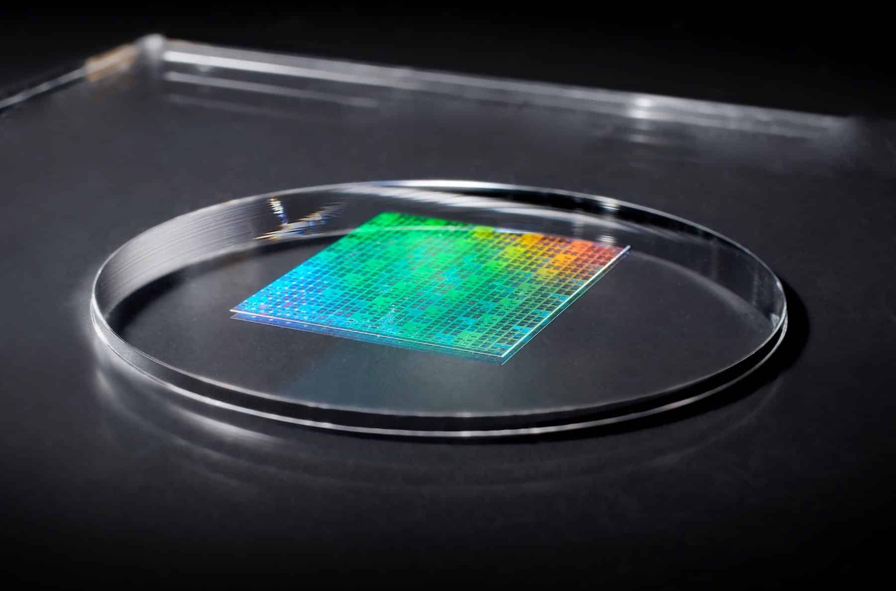
The race towards the most advanced nodes has been marked for years by one word: EUV. Extreme Ultraviolet Lithography has become the most expensive — and energy-intensive — bottleneck in cutting-edge chip manufacturing. That’s why every time a minimally credible alternative appears, the market takes note.
This week, Dai Nippon Printing (DNP) has introduced a new piece to the puzzle: a template for nanoimprint lithography (NIL) capable of transferring patterns with 10 nm lines, which the company associates with processes equivalent to 1.4 nm generation. DNP claims its goal is mass production by 2027 and even sets a commercial target: increasing NIL sales to 4 billion yen in the fiscal year 2030.
The news doesn’t come alone. Canon, which has been advocating nanoimprint as a “parallel route” to EUV for years, announced in 2024 that it shipped its first commercial FPA-1200NZ2C system to the Texas Institute for Electronics (TIE), with a message directly targeting fab financials: lower energy consumption and reduced tool costs compared to traditional exposure methods.
Why does this matter to a financial media outlet
In semiconductors, technological leaps matter… but what moves the market is capex + opex + risk:
- Capex (investment): EUV and, especially, the jump to High-NA EUV raise figures to levels only a few can handle. The public conversation around High-NA has already normalized figures around $350 million per machine in the industry following ASML’s ecosystem.
- Opex (energy and operations): the electric cost of an advanced factory isn’t a detail; it influences site selection, supply agreements, and expansion limits. The industry has long accepted that EUV is a “heavy” energy consumer, and TSMC, for example, has announced specific initiatives to reduce peak energy consumption of its tools and processes.
- Risk (performance and defects): any alternative is only viable if it doesn’t compromise yields, break layer alignment, and scale to volume.
Within this context, NIL’s promise isn’t “replace EUV,” but more pragmatically: take over some work.
What exactly is DNP announcing (and where’s the “value”)
DNP claims to have developed a NIL template with a 10 nm line pattern, leveraging techniques like Self-Aligned Double Patterning (SADP) and combining mask-making expertise with manufacturing process technologies.
The financial key lies in two statements from the announcement:
- “It can replace part of the EUV process” (not the entire flow).
- In energy savings, DNP states that NIL could reduce exposure process energy consumption to about one-tenth compared to readily available processes like ArF immersion and EUV.
If such savings are reproducible in real production (which remains a big “if”), the impact would be twofold: lower direct electricity costs and potentially less need for EUV-capable capacity for certain layers.
Canon supplies the machine; DNP supplies the “mold”: a value chain reading
Canon is trying to reposition itself in a segment historically dominated by the optical lithography duopoly/tripoly, with ASML in EUV as the unavoidable reference. Canon’s 2024 announcement was clear: its commercial NIL tool was delivered for R&D at the TIE and is marketed as an energy-efficient and lower-cost alternative to optical projection systems (including EUV), though initially better suited for research and validation phases.
From a financial perspective, this paints a thesis of “optionality”:
- DNP seeks to monetize its pattern/template expertise and become a critical supplier if NIL scales. It also sets sales targets for 2030, suggesting it doesn’t see this as a marginal experiment.
- Canon gains relevance in a market where lithography tool spend is among the most strategic in fab capex, though entering mass production remains a high hurdle.
For the market, the key point is that NIL doesn’t need to replace EUV entirely to have an economic impact: it’s enough if it’s used on some layers where overlay/defect tolerances are more flexible.
The brake: the reality of volume manufacturing
This is where corporate optimism meets the “investment committee” of foundries.
DNP talks about evaluations with manufacturers and a mass goal of 2027. But the big question — and the one that impacts valuation the most — remains the same as for NIL for years:
- Defectivity: a stamping process can introduce defects through particles, contamination, or template wear.
- Template lifespan: if the “mold” degrades quickly, operational costs soar and become unpredictable.
- Layer alignment (overlay): at advanced nodes, error margins are measured in mere nanometers; maintaining that with physical contact is a significant challenge.
- Industrial cadence: even with improvements, throughput must align with a 24/7 wafer-per-hour fab.
In other words: the proposition is attractive for cost reduction, but only if it doesn’t impose an invisible tax on yields, quality, and cycle time.
Can it shift the needle for ASML and the EUV “trade”?
In the short term, the most realistic scenario isn’t “Canon versus ASML,” but NIL as a complementary tool.
Furthermore, High-NA EUV isn’t just a technological issue; it’s a matter of capex planning over many years, with machines costing hundreds of millions and supply chains already committed.
If NIL thrives, the financial impact could come through three channels:
- Less incremental EUV capex pressure on specific layers (not across the entire process).
- Lower wafer-level electricity costs at certain steps.
- Increased bargaining power for foundries in tool mix—something rarely seen in cutting-edge lithography.
If it doesn’t succeed, the simple interpretation is that it will be another promising technology that failed to bridge the gap from lab to fab.
What investors and analysts will monitor in 2026–2027
In this type of story, the “event” isn’t just the announcement; it’s the commitment signal from a foundry. Therefore, the market will watch:
- Who validates NIL on specific layers and with what measurable results (defects/yield).
- Whether recurring supply agreements emerge (not just pilot projects).
- Whether the discourse shifts from “potential savings” to “proven reduction of EUV steps” in actual flows.
- Whether DNP’s 2027 target is accompanied by industrial expansion and contractual commitments.
For now, what exists is a promise with a timeline, and two Japanese companies aligning product (machine + template) to tackle the biggest pain point in advanced lithography: cost and energy.
via: global.dnp