The idea sounds like a techno-spy movie: an underground lab in China, pieces recovered here and there, engineers working under false identities, and a goal that has captivated half the industrial planet: to build an Extreme Ultraviolet (EUV) lithography machine capable of producing cutting-edge chips without relying on the West. But the reality, for now, is much less epic and far more prosaic. According to the latest information and analysis published in specialized media, the so-called EUV “reconstructed” by China has not produced a single chip, and at best, it remains an experiment that will take years to approach operational use.
The starting point is a Reuters report describing a covert state effort to develop a proprietary EUV lithography system: a kind of “Manhattan Project” for semiconductors, aiming to break the bottleneck that bothers China most after years of sanctions and export controls. The key element of the story is that the prototype purportedly achieved generation of EUV light, a significant technical milestone. The problem is: generating EUV light does not mean manufacturing chips. The prototype, as described, is far from achieving the performance, precision, and stability needed for real production environments.
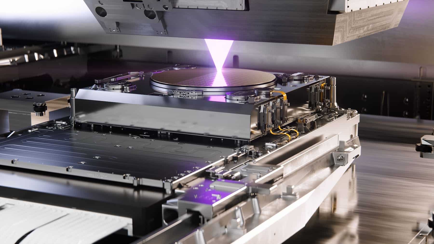
The Great Misunderstanding: In EUV, Having a Light Source Is Not Enough
In popular imagination, an EUV machine is reduced to “a very special light” that allows tiny patterns to be inscribed onto a wafer. In reality, it’s an ecosystem inside a box: precision optics, ultrafine movement, extreme vacuum, metrology, thermal control, proprietary software, and a choreography of subsystems that must operate continuously for weeks in a manufacturing setting. It’s not a single device but an integration of tens of thousands of parts and tolerances that border on the unbelievable.
Moreover, EUV light has an inconvenient characteristic: it’s easily absorbed. That’s why lenses like those in DUV lithography are not used; instead, multilayer mirrors inside vacuum chambers reflect the EUV radiation. Every detail is crucial—from how the beam is stabilized to how pattern distortion is minimized when operating at industrial speeds.
This is the crux of recurring criticism: the Chinese “Frankenstein” might have been assembled from components acquired through indirect channels—spare parts, old equipment, refurbished components—but that doesn’t make it a ready-to-use manufacturing tool. Not even that it functions at a basic level.
Why “Stealing a Blueprint” Doesn’t Work: There Is No Single Blueprint for an EUV
Another point that dismantles the quick-copy narrative is the origin of modern EUV machines, dominated by ASML. It’s not a product that emerges from a single building with one master blueprint. It’s the result of distributed development, with critical suppliers across the U.S., Europe, and Japan, and decades of iteration to turn fragile subsystems into a platform suitable for high-volume manufacturing.
The EUV source now standard in industry relies on a method called LPP (Laser-Produced Plasma): a CO₂ laser pulses on tiny tin droplets to generate EUV radiation at 13.5 nm. It’s an extremely demanding system, because turning it on is not enough: it requires stable power, minimal debris, controlled wear, and reproducible operation. Above all, the EUV light must reach the rest of the machine with the quality required for production.
In ASML’s case, a key detail is the Cymer division (acquired by ASML), which develops the EUV light source. The high-precision optical system depends on Carl Zeiss SMT, the leading manufacturer of EUV mirrors and optics. Zeiss describes its EUV projection optics as a set of six mirrors and around 20,000 parts weighing approximately 2 tons, all with extreme requirements to reproduce structures of just a few nanometers on the wafer. In other words: even with access to individual components, replicating the core optical system is an enormous barrier.
The Real Bottleneck: Optics, Mechanical Stages, and Software
Published details suggest that the Chinese prototype struggles in critical subsystems: precision optics, mechanical stages, and other components that must move with nanometric accuracy and repeat millions of times without degradation. Reuters sets the political goal to produce prototype chips by 2028, though sources cited in the same report consider 2030 a more realistic timeline.
Even if the hardware were more or less assembled, another obstacle emerges: software and firmware that coordinate the system. Advanced lithography machines do not behave like generic computers running any operating system. Control software is integral to the product, involving calibrations, diagnostic routines, and compensations built over years, based on real data from actual factories. Without this accumulated knowledge, a physical tool—even if assembled—may be unusable.
An Uncomfortable Conclusion: Modularity Opens Doors… But Doesn’t Deliver a Complete EUV System
The analysis also offers a harsh reality for Western industry: modularity and the parts market can allow third parties to obtain pieces or data. Chinese manufacturers, for instance, are said to have improved DUV capabilities by sourcing components from third parties, stretching existing tools to produce more demanding nodes. Such tactics do not require “perfect EUV”: improving performance or yield by even 10% can be profitable under restrictions.
But EUV is a different level. The difference between “assembling a light-emitting setup” and “producing chips reliably” is the difference between a laboratory experiment and an industrial process.
Years Away from Actual Production, Even if the Prototype Exists
The overall message is not that China “cannot” advance, but that the journey is longer than viral headlines suggest. EUV lithography is largely a supply chain turned into technology: materials, optics, metrology, vacuum, control, integration, training, maintenance, and accumulated expertise. And that chain, by design and by geopolitical realities, remains fragmented.
Thus, the “Frankenstein” becomes a fitting metaphor: an assemblage of parts that can impress with its ambition but is not yet an industrial tool. In the short term, the real impact is unlikely to be China’s immediate production of advanced EUV chips, but rather that supporting such a project reinforces a broader trend: the semiconductor race is becoming a contest of technological sovereignty, public investment, and strategic patience.
Frequently Asked Questions
What exactly is EUV lithography, and why is it so critical for advanced chips?
EUV (extreme ultraviolet) is a lithography technology that uses 13.5 nm wavelength light and vacuum optics to print extremely fine patterns. It’s essential for manufacturing the most advanced nodes, enabling higher density, lower power, and better performance.
Why can’t a prototype that “generates EUV light” automatically produce chips?
Because the light source is only one part of the equation. Without precision optics, mechanical stages, stable vacuum, metrology, and control software, the machine cannot transfer patterns with the accuracy and repeatability required for production.
What roles do Cymer and Carl Zeiss play in ASML’s EUV machines?
Cymer (part of ASML) develops the EUV plasma light source, while Carl Zeiss SMT manufactures the ultra-precise optics and mirrors—components that are critical and extremely difficult to replicate.
When might China manufacture chips with its own EUV system if the project continues?
Public statements target around 2028 for prototypes, with more realistic estimates around 2030. However, achieving large-scale manufacturing typically takes longer than developing a proof-of-concept chip.