
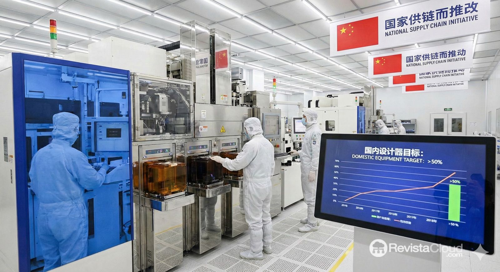
China’s Empyrean Technology says it has cut the time needed to complete a circuit design task from four weeks to one using agentic artificial intelligence. The 75% improvement, announced by its chairman, Liu Weiping, applies to a specific simulation and layout flow, so it doesn’t mean the company can design an entire chip four times faster. The advance is significant because Empyrean develops electronic design automation (EDA) tools, one of the pieces of the semiconductor industry where China is trying to reduce its dependence on foreign technology.
Agentic AI in chip design: the key points in 30 seconds
- Empyrean says an AI agent cut a specific circuit design task from four weeks to one.
- The Chinese company is also working on an agent-based EDA platform, according to Liu Weiping, speaking in Shenzhen.
- EDA tools are involved in stages such as design, simulation, verification, and physical layout of circuits.
- Synopsys and Cadence are also developing agentic workflows to automate parts of semiconductor design and verification.
- For China, these tools carry extra value: building a domestic EDA industry reduces its dependence on US suppliers.
Liu’s remarks came during the International Integrated Circuit Innovation Expo 2026, held in Shenzhen, and were reported by the South China Morning Post. The executive explained that Empyrean is introducing AI-optimized algorithms and agents capable of operating its own simulation and design tools.
The difference from simply bolting a chatbot onto an engineering program is significant.
An agent can receive a goal, decide which tools it needs, execute different steps, interpret the results, and repeat part of the process until certain conditions are met. The engineer still defines the goals and reviews the work, but part of the intermediate operations can be automated.
This is especially attractive in semiconductor design, because creating a modern chip requires continuously running different tools, checking results, and going back whenever a change introduces new problems.
What an AI agent can actually do inside an EDA tool
EDA stands for Electronic Design Automation.
These tools are the software engineers use to turn a chip architecture into a design that can ultimately be manufactured. They come into play in processes such as logic description, synthesis, verification, simulation, placement, routing, and physical design checks.
They are not the machines that physically manufacture the chips.
This distinction matters because EDA tools are sometimes confused with the lithography equipment used later on in semiconductor fabs.
| Stage | Example tools or processes |
|---|---|
| Architecture | Defining functions and blocks |
| RTL | Logic description of the circuit |
| Verification | Checking that the design works |
| Synthesis | Converting RTL into logic gates |
| Placement | Physically placing the elements |
| Routing | Creating their interconnections |
| Sign-off | Checks before manufacturing |
| Fabrication | Physical production on the wafer |
Empyrean works on the software side of this chain.
The experiment described by Liu used an agent running on simulation and layout tools. According to the executive, a task that previously took four weeks could be completed in one.
That represents a 75% reduction in time or, put another way, a process four times faster.
But it doesn’t allow us to conclude that Empyrean has cut the total time needed to develop a processor by 75%.
Designing an advanced semiconductor can take years and requires large teams working simultaneously on architecture, logic, memory, interfaces, verification, physical design, and validation.
Empyrean’s figure applies to one specific task, and it also comes from the company itself. So far, not enough technical information has been published to independently reproduce that test.
AI agents are moving into the entire EDA industry
China is not alone in this direction.
Two of the world’s largest semiconductor software companies, Synopsys and Cadence, have unveiled systems during 2026 that use agents to automate processes traditionally carried out by engineering teams.
In March, Synopsys unveiled AgentEngineer, a technology based on multiple coordinated agents.
The demonstration includes a flow capable of generating Register Transfer Level (RTL) code from specifications, running checks, generating testbenches, and iteratively running verification tools until it approaches the set targets.
Synopsys says it has observed productivity gains of two times and up to five times in certain cases. These are results reported by the company and depend on the specific flow and design analyzed, so they can’t automatically be extrapolated to any project either.
In July Synopsys expanded this strategy with Microsoft and AMD. One of its autonomous debugging flows showed, according to the company, a reduction of up to 40% in cycle time.
The company has also worked with Nvidia on verification agents. In another demonstration, it reported up to 50 times less time to reach validated RTL and an additional 20% in coverage.
Cadence is following a similar direction.
In June it unveiled its ChipStack AI Super Agent, which the company describes as a virtual engineer with a high level of autonomy. Nvidia is using its technologies to run large numbers of simulations related to design verification.
Cadence says certain flows can achieve RTL validation cycles more than 40 times faster and cut a typical five-week process down to less than a day.
Again, these are results provided by the vendors under specific scenarios. A direct comparison between Empyrean’s 75%, Synopsys’s 40%, or Cadence’s figures wouldn’t be accurate, because they aren’t necessarily measuring the same task, design, or methodology.
What matters is the shared direction.
| Company | 2026 development announced |
|---|---|
| Empyrean | Agents applied to simulation and layout |
| Synopsys | Multi-agent flows for design, verification, and debugging |
| Cadence | ChipStack AI Super Agent |
| AMD | Evaluating agentic flows developed with Synopsys and Microsoft |
| Nvidia | Use of, and collaboration on, automated design and verification flows |
Generative AI is thus moving from helping engineers look up documentation or write snippets of code to directly operating professional tools within multi-step workflows.
Why EDA matters so much to China
For Beijing, there’s another reason to accelerate this technology.
The global EDA market has historically been highly concentrated around a handful of companies, especially Synopsys, Cadence, and Siemens EDA.
China has chipmakers such as Semiconductor Manufacturing International Corporation (SMIC) and is developing domestic suppliers of equipment, materials, and memory. But manufacturing competitive semiconductors requires mastering a much broader chain than the fab itself.
Design software is one of those dependencies.
A modern processor contains billions of transistors. Designing it by hand is impossible, so EDA tools are needed to automate much of the work and verify that the design can actually be manufactured.
In recent years, the United States has used export controls on various semiconductor technologies bound for China, temporarily including some EDA products during 2025 — a restriction Washington would later lift in exchange for rare earths, although other controls related to advanced chips and manufacturing equipment remain in place.
That experience reinforced China’s interest in having its own alternatives.
Empyrean, which previously launched China’s first full-process EDA platform for memory, is among the companies Beijing considers important for building that technological self-sufficiency.
Agentic AI could help in two ways. It can improve engineers’ productivity and, at the same time, allow domestic tools to progress faster in certain workflows.
That doesn’t mean adding agents immediately closes the gap with international leaders.
EDA software needs decades of development, huge amounts of specialized know-how, and a close relationship with semiconductor fabs and their manufacturing processes. A tool’s accuracy is especially important, because an error caught after masks have been produced and the first wafers manufactured can be extremely costly.
An agent can work faster, but it can also get things wrong faster
Applying generative models to electronic design also presents a different problem than generating text or images.
An incorrect chatbot response can be annoying. An error in a semiconductor design that isn’t caught before manufacturing can have far greater financial consequences.
That’s why automation needs to be paired with verification.
Agents can generate RTL, launch simulations, analyze errors, tweak parameters, or try to optimize power, performance, and area. But the results still have to go through deterministic verification tools and engineers’ validation processes.
AI’s usefulness lies precisely in reducing the number of manual operations needed to reach a valid design, not in replacing physical and logical checks.
This sets the use of EDA agents apart from many enterprise AI applications.
The agent can’t just settle for “answering correctly.” It has to produce results that ultimately satisfy mathematical, electrical, physical, and manufacturing constraints.
China is also turning AI into industrial policy
Empyrean’s statements coincide with a new phase of Chinese technology policy.
The Ministry of Industry and Information Technology (MIIT) published its development plan for the information and communications sector for the 2026-2030 period on September 7.
The document places AI integration among the priorities for technological modernization and complements the previously announced “AI + Information and Communications” program for 2026-2028.
The official goal includes developing compute infrastructure, more autonomous networks, and agent-based industrial applications. By 2028, MIIT wants to have more than 30 high-value scenarios and various specialized agents within the information and communications sector.
EDA is part of an even broader industrial issue: using AI to cut the time needed to develop other technologies.
That could create an interesting effect in the semiconductor race.
In recent years, a large part of the AI competition has focused on building better chips to train artificial intelligence. The next phase is starting to work in the opposite direction too: using artificial intelligence to design better chips.
If agents manage to consistently cut the weeks spent on some verification, simulation, and physical design tasks, the advantage won’t simply be needing fewer engineers. Teams could test more alternatives within the same schedule, catch errors earlier, and spend more time on the difficult decisions that still require specialists.
Empyrean has shown a concrete example with a reduction from four weeks to one. Synopsys and Cadence are reporting similar results in other parts of the process.
It remains to be seen how much of these improvements holds up when agents are used continuously on full projects and highly complex chips.
But the direction is already clear: the AI race and the semiconductor race are starting to merge. China needs better tools to design its own chips, and it’s trying to use artificial intelligence to speed up precisely the development of that capability.
