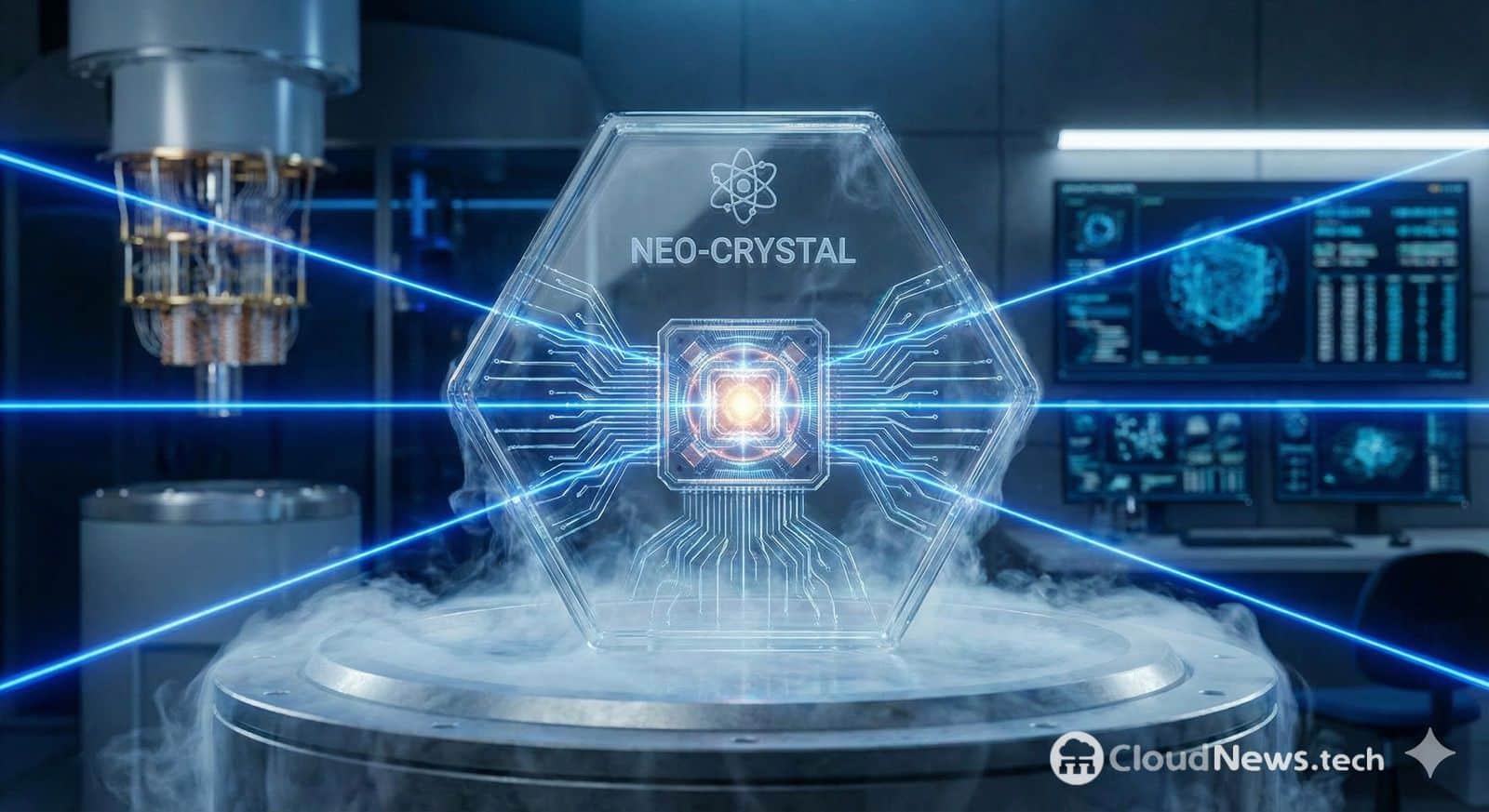
China has decided to fully engage in one of the most strategic—and least visible to the general public—fronts of the semiconductor industry: glass substrates. This emerging technology aims to replace part of the traditional organic materials in advanced packaging of chips, a critical area for scaling AI processor performance without increasing power consumption, heat, or mechanical distortions of the package.
According to sector information collected in Asia, Visionox, one of China’s leading display manufacturers, is preparing investments and a supply chain geared toward this new business. It is not alone: the Chinese PCB manufacturer AKM Meadville reportedly has set up a pilot line for this type of substrate, while the assembly and testing company Tongfu Microelectronics is building its own supplier network to position itself in a market where packaging will be as crucial as silicon itself.
The coordinated entry of companies with very different profiles (displays, PCBs, and OSAT) reveals a shared outlook: the race for the next generation of AI chips will not only be fought at manufacturing nodes but also in materials, interconnection, and substrates. And glass, thanks to its physical properties, has become a candidate with the potential to push beyond the limits that organic substrates are starting to reach.
Why “Glass” Matters in the AI Era
The concept may sound counterintuitive: what does glass have to do with modern computing? In packaging, the substrate acts as an interconnection platform and support. As chips grow larger, with more memory and high-speed links, the challenge shifts from merely “making transistors” to connecting and stably maintaining a massive, dense assembly.
The glass substrate (often referred to as glass core substrate or variants with via structures through the glass) promises advantages in flatness, thermal stability, and deformation control over organic solutions—key aspects when seeking finer interconnects and larger packaging areas. However, these promises coexist with significant industrial challenges: glass requires extreme process controls to prevent defects like microcracks, as well as hurdles in handling, drilling, and metallization.
The growth expectation is supported by a simple fact: AI is driving the development of more complex chips with more ambitious packaging, and the market is seeking alternatives that can increase density and reliability without multiplying costs and assembly risks.
China’s Moves: Visionox, AKM Meadville, and Tongfu Enter the Scene
In this context, China has begun shifting pieces. Visionox, traditionally associated with display technology, is reportedly preparing investments in glass substrates as a “new growth engine,” after months spent configuring an ecosystem of materials, components, and equipment. Meanwhile, the PCB manufacturer AKM Meadville—active in high-density interconnection segments—has set up a pilot line to accelerate its entry into supply, and Tongfu Microelectronics, renowned in the OSAT sector and connected to China’s tech supply chains, is strengthening its positioning to compete in next-generation packaging.
The industry interpretation is clear: it’s not just about “participating,” but about controlling more of the value in an era where advanced packaging is capturing increasing relevance (and margins) within the semiconductor chain. Additionally, the transition from display companies to semiconductors reflects another trend: with the modest growth of displays, several Asian players are seeking the next value leap in adjacent industries where they already dominate large-scale glass processes.
Another sign of ambition is the “big bang” approach: rather than attacking a single link, some industry sources suggest that new Chinese entrants aim to deploy the entire supply chain quickly, betting on financial strength, rapid execution, and volume to gain price competitiveness once the technology stabilizes.
A Global Race with Established Players in Korea, Taiwan, Japan, and the US
The Chinese movement is not targeting an empty market. The race for glass substrates has been heating up for some time among South Korea, Taiwan, Japan, and the United States.
- In South Korea, initiatives around Absolics (a subsidiary linked to SKC with industrial plans in the US) are emerging, and Samsung Electro-Mechanics has publicly shown activity related to glass core materials and agreements. Likewise, LG Innotek has been mentioned in Asian media as participating in this technological race.
- In Japan, companies like DNP have announced progress on pilot lines for substrates with via-through-glass (TGV) technologies, aiming to validate production and send high-quality samples.
- In Taiwan, interest intersects with the leadership in packaging and substrate ecosystems, with companies like Unimicron frequently discussed regarding deformation control and assembly processes on glass.
- In the US, the roles of Intel and its associated industrial strategies for advanced packaging make this a key component in the global technological competition.
Overall, the landscape suggests a multinational market from the start, with dynamics of technological sovereignty, supply chain control, and increasing pressure to industrialize rapidly without compromising reliability.
The Bottleneck Isn’t Just Manufacturing: It’s Mastering the Process Without Breaking the Glass
The big question isn’t whether glass “works” in the lab: it’s whether it can be scaled with high yields, consistency, and manageable costs. The sector discusses issues such as microcracks, defects, process complexity, and the need for an end-to-end supply chain (equipment, chemistry, metallization, inspection) to prevent a physical promise from turning into a manufacturing problem.
Thus, China’s entry is seen as an accelerant of competition: if they succeed in quickly integrating the supply chain and increasing volume, they could compel others to accelerate investments, reduce costs, and shorten timelines. Conversely, this pressure could also lead to a “race” where technical risks escalate if industrialization advances too quickly.
What is clear is that glass substrates are no longer just a curiosity—they have become a strategic front for AI-oriented chip packaging. With China entering the arena, the contest promises to become more intense, faster, and potentially more decisive for the hardware landscape of the coming decade.
Frequently Asked Questions
What is a glass substrate in semiconductors and what is it used for?
It is an alternative to organic substrates in chip packaging. It functions as an interconnection platform and physical support, aiming to improve flatness, thermal stability, and deformation control in advanced packaging.
Why are glass substrates associated with AI chips?
Because AI drives larger, more complex chips with more interconnects and thermal demands. Glass is being studied as a way to support higher density and stability in advanced packaging.
What technical challenges hinder widespread adoption of glass substrates?
Microcracks, material handling, process complexity such as via-through-glass (TGV), metallization, and large-scale quality control.
Which companies are competing to lead this technology?
Besides new Chinese players (Visionox, AKM Meadville, Tongfu Microelectronics), initiatives are emerging in Korea (Absolics, Samsung Electro-Mechanics, LG Innotek), Taiwan (linked to Unimicron), Japan (DNP), and the US (Intel).