Cadence and Intel Foundry have expanded their collaboration to accelerate the optimization of Intel 14A process, one of the next-generation manufacturing technologies that Intel aims to strengthen its business as a foundry for third parties. This multi-year agreement will focus on technology and design co-optimization, IP availability, and customer-oriented design tools for chips used in high-performance computing and mobile devices.
The move comes at a particularly sensitive time for the semiconductor industry. Advanced nodes no longer rely solely on manufacturing capacity. They also demand design tools, libraries, verified IP, mature methodologies, and production-ready PDKs. Without this ecosystem, a process may look promising on paper but be difficult for external customers to adopt.
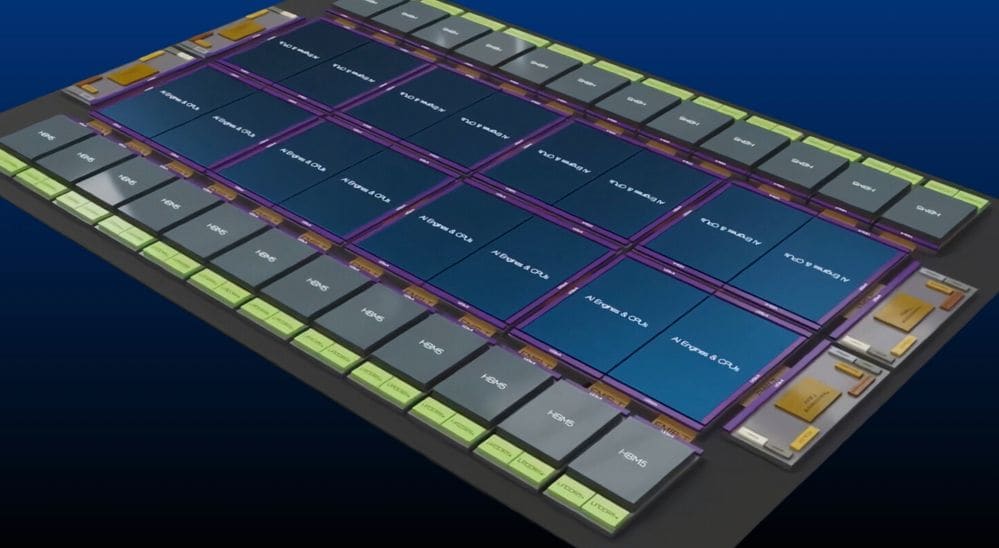
Intel 14A needs more than just good process technology
The collaboration will be supported by DTCO, short for Design Technology Co-Optimization. In practice, this means that chip design and manufacturing technology are jointly refined from early stages to improve performance, power consumption, and area—the three variables that the industry summarizes as PPA.
Cadence will contribute its EDA tools, AI-driven flows, and design IP solutions. Intel Foundry will provide its process technology, packaging capabilities, and advanced design experience. Both companies will work together to optimize tools, flows, and methodologies with the goal of delivering Intel 14A PDKs ready for production.
This is a key point. A PDK, or Process Design Kit, is the package that enables designers to create chips compatible with a specific process. It includes design rules, electrical models, libraries, and other elements necessary to turn an idea into fabricatable silicon. At advanced nodes, the maturity of the PDK can directly influence time-to-market.
| Collaboration Area | Cadence’s Contribution | Intel Foundry’s Contribution |
|---|---|---|
| DTCO | Design tools, flows, and methodologies | Process technology and manufacturing criteria |
| PPA | Performance, power, and area optimization | Node tuning for real workloads |
| PDKs | Integration with EDA tools | Provision of production-ready kits |
| Design IP | Reusable building blocks to accelerate projects | Compatibility with Intel 14A |
| AI-driven | Automation of design flows | Co-optimization with process and packaging |
| End customers | Reduced design risk | Foundry capabilities for HPC and mobile |
Why it matters for HPC and mobile markets
Cadence and Intel explicitly mention two target areas: HPC and mobile design. Although they are different markets, both face common pressures. They require higher performance per watt, increased density, and tighter design cycles. In high-performance computing, improvements can come from processors, accelerators, chiplets, memory, interconnects, and advanced packaging. In mobile, every square millimeter and millivolt count.
Competition in these markets is not solely about smaller transistors. Design teams need tools that allow them to explore options, reduce iterations, catch issues early, and adapt chips to the process. AI applied to EDA can assist in this effort, but it’s important not to see it as a magic solution. Its value lies in speeding up analysis, automating repetitive decisions, and reducing risks during phases where errors could cost months.
Anirudh Devgan, President and CEO of Cadence, described the expansion of the relationship with Intel as a milestone for both companies. According to him, the collaboration aims to help customers achieve new levels of performance, power efficiency, and productivity, as well as accelerate the realization of next-generation products.
Naga Chandrasekaran, Executive Vice President and General Manager of Intel Foundry, positioned the agreement within Intel’s effort to meet its technological roadmap and strengthen its ecosystem. He highlighted the combination of Intel’s process and packaging capabilities with Cadence’s AI-driven design tools.
The challenge for Intel Foundry: building trust in the ecosystem
For Intel Foundry, alliances like this are crucial because third-party manufacturing business requires more than just industrial capacity. Customers need confidence in the roadmap, availability of tools, IP support, and stable delivery timelines. A foundry competes not only with wafer capacity but with an entire ecosystem.
TSMC has built an advantage over years, not only on manufacturing but through a vast network of EDA, IP, packaging, validation partners, and customers. Samsung Foundry also seeks to strengthen its position with advanced nodes and ecosystem support. Intel, which has historically mostly manufactured for itself, needs to demonstrate that it can operate with the discipline, openness, and predictability that external designers expect.
The partnership with Cadence supports this goal. As one of the leading companies in EDA, alongside Synopsys and Siemens EDA, Cadence’s tools are widely used in chip design flows. If Intel 14A reaches the market with solid support in widely adopted design platforms, the barrier to adoption for potential customers may be lower.
| Intel Foundry Challenge | How Cadence Can Help |
| Attract external customers | Reduces design barriers in familiar tools |
| Mature Intel 14A | Facilitates co-optimization of process and design |
| Deliver production-ready PDKs | Speeds up validation and readiness for manufacturing |
| Compete with established foundries | Strengthens the ecosystem around the node |
| Reduce customer risk | Enhances predictability in complex flows |
| Capture HPC and mobile designs | Provides IP and methodologies for demanding markets |
AI enters chip design, but value lies in integration
Cadence positions its offering as part of its AI-powered EDA and IP solutions. The term reflects a clear trend: electronic design automation tools are incorporating more advanced automation to assist with tasks like architecture exploration, physical optimization, verification, timing closure, and power analysis.
In advanced chips, each new generation increases complexity. Design teams need to coordinate architecture, logic, memory, interconnection, power, packaging, thermal, and manufacturing aspects. AI can help navigate this space, but the outcome depends on data quality, process rules, and integration with existing tools.
Therefore, the collaboration makes sense from an industry perspective. Cadence isn’t working in isolation on a generic tool; it will collaborate with Intel Foundry to adapt flows, methodologies, and products for Intel 14A. This close partnership between EDA provider and foundry can reduce friction as customers start deploying real designs in the node.
The promise of faster time-to-market and reduced design risk should be taken with caution. Each chip has specific requirements, and adopting a new node always involves complex validation. However, a more mature design platform from the start can make a difference, especially for customers unable to afford multiple delays.
A seemingly small agreement but strategic for Intel
The announcement does not provide economic figures or customer names, but the strategic importance is clear. Intel needs to position Intel Foundry as a serious alternative in advanced manufacturing. Cadence, on its part, wants to ensure its tools and IP are ready for the nodes that could shape the market’s future.
For customers, the key questions will be when production PDKs will be available, which IP blocks will be ready, what performance Intel 14A can deliver in commercial designs, and how the process, packaging, and tools combination compares to established alternatives.
The partnership also reflects how the chip industry is evolving. No longer is it enough for a company to announce a node; the design ecosystem must be capable of reliably supporting it. The semiconductor race is fought not only in factories but also in software, libraries, validation flows, and cross-company agreements that turn process technology into real products.
Cadence and Intel Foundry have strengthened that less-visible but essential part. If Intel 14A aims to compete in HPC and mobile, it will need committed customers, ready tools, and a clear development path from design to production. This agreement does not guarantee node success but emphasizes a crucial priority: making technology designable, verifiable, and market-ready.
FAQs
What have Cadence and Intel Foundry announced?
They have expanded their collaboration to optimize the Intel 14A process through DTCO, EDA tools, Design IP, and AI-driven design flows.
What is Intel 14A?
Intel 14A is a next-generation process technology from Intel Foundry aimed at advanced future designs, including chips for high-performance computing and mobile devices.
What does DTCO mean?
DTCO stands for Design Technology Co-Optimization. It involves jointly optimizing chip design and manufacturing technology to improve performance, power, and area.
Why is this agreement important?
Because foundry customers need mature tools, PDKs, and IP to design chips with lower risk. Collaboration with Cadence can facilitate the adoption of Intel 14A.