In the semiconductor industry, we almost always look at the same thing: Nvidia designs the accelerators that power artificial intelligence; TSMC manufactures for half the planet; Samsung and Intel compete to regain ground in the most advanced nodes; and Apple, AMD, and Qualcomm turn those chips into products that reach pockets or data centers.
But behind all of them, there is a less publicly known company that holds a much more delicate position than it appears. ASML doesn’t make chips. It manufactures the machines that enable the production of the world’s most advanced chips.
The Dutch company, founded in 1984 as a joint venture between Philips and ASM International, has become one of the most critical bottlenecks in the digital economy. Its name no longer functions as an acronym, although it originally stood for “Advanced Semiconductor Materials Lithography.” Today, ASML is simply ASML: a Veldhoven-based company that designs and produces lithography systems for the chip industry.
Its role is as specific as it is decisive. A semiconductor factory can have billions in investment, clean rooms, wafers, chemicals, technicians, robots, and highly advanced inspection processes. But if it wants to produce cutting-edge chips, it needs extreme ultraviolet (EUV) lithography. And in commercial production, that technology has a name of its own.
ASML.
The machine that prints the invisible
Lithography, simplified greatly, is the process that allows printing tiny patterns onto a silicon wafer. These patterns are repeated layer by layer to form a chip’s circuits. The smaller and more precise these features are, the more transistors fit in the same space, increasing computing power, energy efficiency, or performance.
For decades, the industry has been reducing the wavelength of light used to etch these patterns. ASML manufactures DUV (deep ultraviolet) systems, which remain essential for many layers of current chips. But the truly challenging leap came with EUV: 13.5-nanometer light so extreme that it behaves awkwardly with almost everything we know in industrial optics.
Generating this light seems like science fiction. The system fires tiny molten tin droplets inside a vacuum chamber. A CO₂ laser hits them twice: first to deform them, then to vaporize them into a plasma that emits EUV light. This occurs tens of thousands of times per second. The resulting light cannot pass through conventional lenses because nearly all materials absorb it. Instead, it is guided by multilayer mirrors with extremely precise surfaces.
From there, the light travels within the system, reflects off a mask with the chip pattern, and eventually projects onto the wafer. Everything happens in a vacuum, with nanometer-scale thermal, mechanical, and optical control. The machine isn’t just an expensive tool; it’s a fusion of physics, software, mechatronics, lasers, materials, metrology, robotics, and years of industrial integration.
| Parts of the EUV system | Why it matters |
|---|---|
| Light source | Generates 13.5 nm EUV radiation from molten tin plasma |
| Multilayer mirrors | Replace lenses and guide light that is mostly absorbed by other materials |
| Vacuum chamber | Prevents air from blocking EUV radiation |
| Mask or reticle | Contains the pattern to be printed on the wafer |
| Software and metrology | Correct deviations and control the process at nanometer scales |
| Wafer stage | Moves the silicon with unimaginable precision |
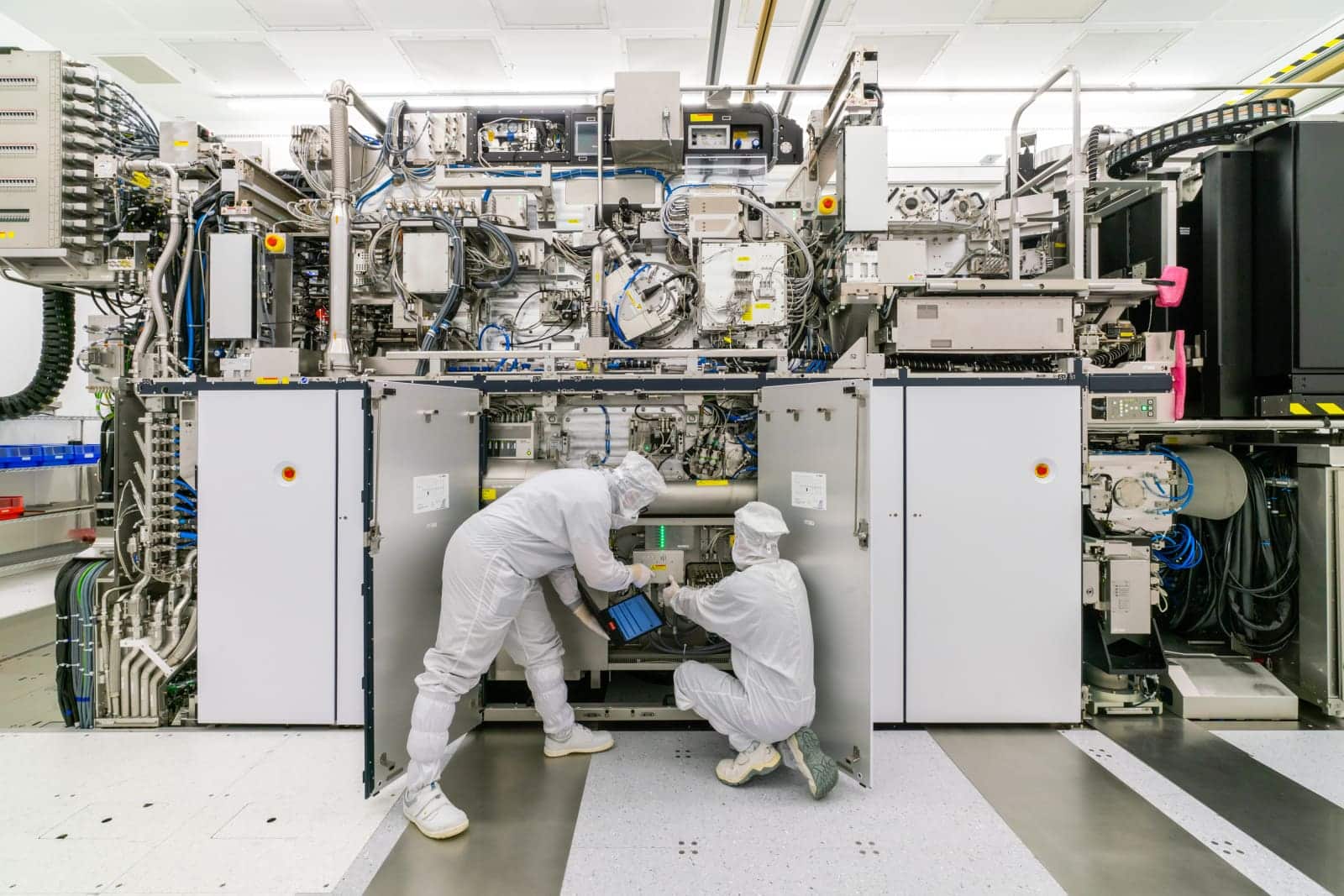
That’s why EUV machines from ASML are often described as among the most complex industrial systems ever built. The phrase might sound exaggerated, but finding many comparable examples is difficult: hundred-ton equipment, with thousands of critical components, transported in dozens of containers, calibrated over months before entering production.
A strange but real monopoly
ASML’s central role in the chip industry didn’t happen by chance. For years, the industry tried to bring EUV from the lab to manufacturing, but the journey was much longer and more difficult than expected. The technology promised to extend Moore’s Law, but generating stable, sufficiently powerful EUV light economically turned into one of the industry’s biggest engineering challenges.
ASML solved this puzzle through a network of highly difficult-to-replicate partners. Notable names include ZEISS, key for precision optics, and Cymer, specialized in light sources and acquired by ASML in 2013. Large customers also played a vital role. Intel, TSMC, and Samsung invested jointly in accelerating EUV development because they knew that without this technology, scaling advanced chips would get much harder.
The result is a very particular technological monopoly. It’s not just about holding patents or a protected machine design. It’s about decades of accumulated knowledge that blends exclusive supplier relationships, integration expertise, factory support, specialized software, and direct ties to the world’s most advanced manufacturers.
| Company | Contribution to the chip ecosystem | Dependency on ASML |
| TSMC | Manufactures advanced chips for Nvidia, Apple, AMD, and other clients | Requires EUV for leading nodes |
| Samsung | Produces advanced memory and logic devices | Uses EUV to compete at the cutting edge |
| Intel | Attempts to regain technological leadership in manufacturing | Among the first to adopt High-NA EUV systems |
| SK Hynix and Micron | Manufacture memory for data centers and AI | EUVe rising in importance for advanced DRAM |
| Nvidia | Designs GPUs and AI Accelerators | Depends on manufacturers with ASML equipment |
Dependency does not mean ASML alone fabricates the future of digital technology. That would be unfair. An advanced chip results from a vast network: designers, foundries, materials, gases, chemicals, EDA software, advanced packaging, memory, energy, ultrapure water, and specialized talent. But ASML holds a singular position because its machine is at the point where design becomes silicon.
And that shifts geopolitics.
Technological power is also in the tools
The chip war isn’t just fought over who designs the best processor. It’s also fought over who controls the essential manufacturing tools. ASML has become a strategic piece for Europe, the US, Taiwan, South Korea, Japan, and China.
China can invest billions in factories, universities, talent, and local companies. But without access to EUV, producing the most advanced chips at scale becomes much more difficult. ASML has publicly stated it has never shipped an EUV machine to China. Export restrictions, mainly driven by the US and enforced through the Dutch government, have made the company an unavoidable actor in global tech policy.
This puts Europe in a curious position. For years, many have said the continent has lost many tech battles to the US and Asia. In consumer electronics, digital platforms, social media, cloud services, or general-purpose processors, that view has some truth. But in one of the most critical tools for manufacturing advanced chips, Europe has a company no one has managed to replace.
ASML is not a consumer platform. It doesn’t show up daily on users’ phones. It doesn’t have Nvidia’s media charisma nor TSMC’s scale. But its influence runs deep because it operates at a layer before: the machines that enable all these companies to exist in their current form.
The next leap is already underway with High-NA EUV, a new generation of machines with greater numerical aperture that will allow even finer details to be printed and reduce process steps in fabrication. These are even more expensive, scarcer, and more complex machines. Intel was one of the first to receive such systems, and other manufacturers are working on adopting them for future chips.
The core message is simple: artificial intelligence, data centers, high-end smartphones, defense systems, electric vehicles, and much of modern electronics don’t only depend on who designs the most eye-catching chip. They also depend on a European company capable of manufacturing the tool that turns those designs into physical reality.
ASML doesn’t produce chips. It produces something possibly more decisive: the industrial capacity to keep producing ever smaller, faster, and more efficient chips. In an economy obsessed with AI models, data centers, and accelerators, it’s worth remembering that it all begins much earlier—in a clean room, with a Dutch machine firing lasers on tiny tin droplets.
Cloud computing, artificial intelligence, and the digital future are also built with mirrors.
Frequently Asked Questions
What does ASML manufacture?
ASML manufactures lithography systems for the semiconductor industry. Its machines enable printing tiny patterns onto silicon wafers for chip production.
Why is ASML so important for artificial intelligence?
Because the most advanced chips used in AI rely on manufacturing processes that use EUV lithography. Without these machines, mass production of many such chips would be much more difficult.
Does ASML make chips?
No. ASML does not manufacture chips or design processors. It sells tools that companies like TSMC, Samsung, Intel, SK Hynix, and Micron use to produce semiconductors.
What is EUV lithography?
It is a chip manufacturing technique that uses 13.5-nanometer extreme ultraviolet light to print very small patterns onto silicon.
Why can’t China buy EUV machines from ASML?
Due to export restrictions related to technological security and strategic semiconductor competition. ASML has publicly stated it has never shipped an EUV machine to China.