The Dutch company ASML has recently revealed the monumental journey that led it to become the sole manufacturer capable of producing extreme ultraviolet (EUV) lithography scanners required to make the world’s most advanced chips. This path involved 20 years of research, an investment exceeding $40 billion, and an unmatched global network of suppliers. In contrast, China remains about two decades behind, according to the latest Goldman Sachs report, trapped in a technological and geopolitical bottleneck that threatens to widen in the coming years.
Twenty Years of Progress, from 65 nm to 2 nm
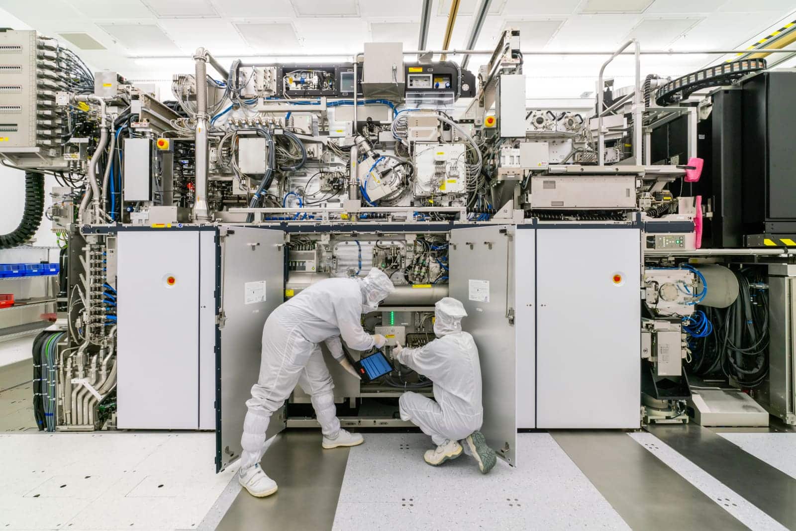
ASML presented a timeline that starkly illustrates the effort invested:
- 2003: Use of ArF Dry lithography at 193 nm, which was sufficient at the time to manufacture chips at 65 nm.
- 2007: Introduction of immersion ArF at 193 nm, enabling scaling down to 28 nm.
- 2017: Introduction of EUV at 13.5 nm, opening the door to 7 nm and 5 nm nodes, which became established between 2019 and 2020.
- 2023: Launch of EUV High-NA systems with a higher numerical aperture, paving the way toward 2 nm and even smaller nodes.
Each transition involved cutting-edge laboratories, failed prototypes, and billions of dollars invested to perfect processes that are impossible to replicate without a highly specialized global ecosystem.
As a result, today each EUV High-NA machine costs nearly $400 million, a staggering price only major manufacturers—such as TSMC, Intel, or Samsung—can afford.
China Still at the Starting Line
Meanwhile, China’s semiconductor industry has failed to produce even a functional prototype of an EUV scanner. Despite patent filings and supposed demonstrations, there is no public evidence of a system similar to that of ASML.

Local manufacturers like SMIC must rely on older DUV technologies, resorting to costly alternative methods to produce 7 nm or even 5 nm chips. Although these achievements make headlines, the reality is that the efficiency and scalability of these processes fall far short of what EUV lithography can offer.
According to Goldman Sachs, China is at the same stage ASML was in 2003, which amounts to a 20-year delay. The European company’s CEO was slightly more cautious, estimating the gap at about 10 years, but analysts generally agree that a significant distance remains to be closed.
The Geopolitical Barrier
The gap isn’t solely due to talent or investment shortfalls in China. It’s a structural problem: advanced lithography depends on a global network of suppliers that includes critical components designed in Europe, the U.S., South Korea, and Japan.
Washington controls much of these strategic exports. Sanctions against companies like SMIC block access to ASML equipment and thwart Beijing’s efforts to catch up. Every new U.S. veto—done in coordination with the Netherlands and Japan—strengthens the technological blockade limiting China’s access to essential EUV lithography components.
The Gap Could Widen
Even if China achieves significant lithography advances before the decade’s end, the pace of global innovation works against it. While Beijing struggles to reach EUV, ASML and its partners are already working on High-NA systems and technologies for nodes of 1.4 nm and smaller.
The risk for China is that instead of closing the gap, it might widen even further. Additionally, producing chips economically without access to modern equipment is challenging: using outdated tools raises costs and hampers industrial scalability.
More Promises Than Results
Official statements from Beijing about imminently developing a domestically produced scanner have so far been mere hype. There are no market products or verified prototypes demonstrating progress comparable to ASML’s.
Experts agree that China faces more hurdles than it admits. If it doesn’t make a real leap in EUV lithography before 2030, Western alliances could solidify a near-absolute dominance in the most advanced nodes.
Conclusion: The West’s Major Technological Blow
ASML’s monopoly on EUV lithography is today one of the West’s greatest strategic victories in its contest with China. No matter how much Beijing invests, without access to the global supplier network and under increasing sanctions, mimicking Europe’s achievement appears nearly impossible.
The key question is whether EUV technology will become the “master stroke” that halts China’s semiconductor ambitions for decades—an industry considered vital for both national security and global economic supremacy.
Frequently Asked Questions (FAQ)
What is EUV lithography and why is it so important?
It’s a chip manufacturing technique using extreme ultraviolet light (13.5 nm) to print finer, more precise circuits. It enables the production of advanced nodes at 7 nm, 5 nm, and below, essential for modern processors.
Why can’t China produce EUV machines?
Because they require components designed by an international network of suppliers, many under U.S., Dutch, and Japanese control. Sanctions prevent access to critical parts.
What is ASML’s EUV High-NA?
It’s the next generation of EUV scanners with a larger numerical aperture that enhances resolution, enabling chips at 2 nm and below. Each unit costs around $400 million.
Can China close the 20-year gap?
In theory, yes, but practically, it looks very difficult. Even with heavy investments, the lack of access to key components and the rapid advancements in the West make the gap likely to grow.
via: elchapuzasinformatico and X