Dutch company ASML, a key player in the global semiconductor industry, has just made a strategic move: opening its first large-scale training academy in the United States, located in Phoenix, Arizona. The goal is as straightforward to summarize as it is complex to execute: train over 1,000 engineers annually capable of installing, maintaining, and repairing some of the most sophisticated machines on the planet—those that enable advanced chips driving the digital economy.
Amidst the effort to strengthen technological independence and reduce reliance on Asia, this announcement aligns with the wave of investments spurred by the CHIPS Act and major projects by Intel, TSMC, Samsung, and Micron on U.S. soil. Building factories is no longer enough: without qualified personnel, these new plants risk lacking the “brains” needed to operate effectively.
A “Talent Academy” for over 1,000 engineers a year
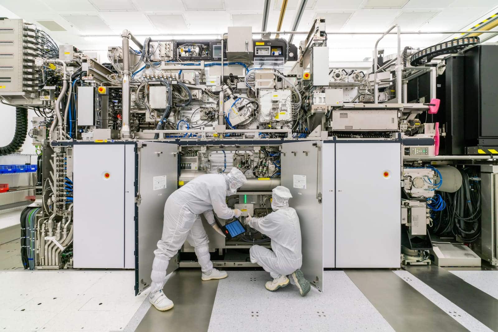
The new center, known as ASML U.S. Technical Training Academy, is just minutes from Phoenix Airport and features 14 classrooms and a cleanroom where students work directly with lithography equipment, including Deep Ultraviolet (DUV) and Extreme Ultraviolet (EUV) systems.
This facility spans approximately 56,000 square feet, or about 5,200 square meters, designed to operate nearly around the clock. The company has engineered the center to run 24/7, with the capacity to train up to 2,000 people annually in the future.
The training programs are not superficial courses. Basic maintenance training for lithography machines lasts between 3 and 6 months, while more complex intervention training takes significantly longer. The academy mainly serves ASML staff but also opens to chip manufacturer engineers working in U.S. fabs, who can pay for training their teams.
Until now, many of these professionals had to travel to Europe or Asia for such advanced training. The Phoenix initiative shifts the landscape, bringing critical knowledge closer to the heart of America’s new manufacturing map.
A direct response to the boom of chip factories in the U.S.
ASML’s decision is best understood within the context of recent years’ ambitious U.S. reindustrialization plans for chips, featuring billions of dollars in grants and credits to attract or expand major fabs.
Some of the most significant projects are concentrated around Phoenix:
- Intel is expanding its presence with new cutting-edge manufacturing lines.
- TSMC, the Taiwanese giants, are building and expanding several high-profile factories in Arizona.
- Samsung is expanding a large plant near Austin, Texas.
- Micron is preparing multimillion-dollar investments in advanced memory.
ASML CEO Christophe Fouquet notes that the opening arrives “at the right moment,” amidst a boom of projects in Arizona and other states like Texas and Idaho competing to attract chip factories. The Phoenix academy thus becomes a supporting pillar for this ecosystem: without enough lithography specialists, these new plants would face greater hurdles to kick off and grow.
Machines as complex as an F-35, with very specific talent requirements
ASML’s machines are not standard industrial equipment. Its most advanced EUV systems cost around $400 million each and require several 747 cargo flights to ship from the Netherlands to customer factories.
ASML Vice President Clayton Patch vividly compares the maintenance of an EUV machine to the level of servicing an F-35 fighter jet. It’s not just electronics: it involves extreme optics, vacuum systems, high-powered light sources, nanometric precision alignments, and system integration approaching aerospace engineering.
Therefore, the company states that many of its top hires come from the military, especially the U.S. Navy and Air Force, where technicians work on highly complex aircraft. Such profiles, familiar with critical systems and strict protocols, fit well with lithography equipment’s demands.
In Phoenix, students will learn on machines that are often prototypes or decommissioned units, rather than brand-new systems destined for clients. This allows hands-on practice without risking delays in delivering new tools or chip production.
A key gap: High-NA EUV training remains in the Netherlands
Despite the scale of the project, ASML maintains some of its most advanced training in Europe. The company has confirmed that, for now, training on its High-NA EUV tools—the latest generation with higher numerical aperture—will continue in the Netherlands, as these systems are still in qualification with clients like Intel and other top manufacturers.
The adoption of High-NA EUV remains limited and not yet in mass production, so centralizing training near R&D and manufacturing hubs is logical from both technical and logistical standpoints. Still, the deployment of standard DUV and EUV systems from Phoenix addresses a significant part of immediate industry needs in the U.S.
Arizona strengthens its role as a key semiconductor talent hub
For Arizona, the inauguration of the ASML academy is also a political and economic victory. Local authorities present it as a further step in establishing the region as one of North America’s main semiconductor hubs, not only in manufacturing capacity but also in specialized talent.
ASML, present in the U.S. since 1984, already employs over 8,500 people in the country—roughly 20% of its global workforce—spread across R&D centers, manufacturing facilities, and close to customer fabs. The Phoenix academy adds a dedicated node for advanced training within this network.
For the U.S. supply chain, this move helps address a major vulnerability identified in recent years: the shortage of highly experienced lithography and advanced equipment maintenance personnel. If America wants its chip reindustrialization efforts to be more than just a series of announcements, infrastructure like this is essential.
A new link in the resilience of the global chip supply chain
The opening of ASML’s Phoenix academy represents more than a corporate gesture; it marks a new phase where technical training becomes central to the resilience of the semiconductor value chain.
While the U.S. works to secure its supply through new factories and Europe promotes its own programs, companies like ASML are now considering not only machinery but entire ecosystems of talent, service, and knowledge.
The fact that the world’s leading maker of advanced lithography systems chooses Arizona for its first major training center in nearly two decades sends a clear message: the future of chips depends not only on cleanrooms but also on the classrooms where future maintenance experts are trained to operate machines day and night for years to come.
Frequently Asked Questions about ASML’s New Academy in Arizona
What is the ASML U.S. Technical Training Academy in Phoenix exactly?
It is an advanced technical training center by ASML, located in Phoenix (Arizona), designed to train over 1,000 engineers annually in maintenance and installation of DUV and EUV lithography equipment. The center has 14 classrooms, a cleanroom, and 24/7 capacity, serving both ASML personnel and chip manufacturer engineers with U.S. factories.
Why did ASML choose Arizona for its first major training center in the U.S.?
Arizona has become a new core hub of the U.S. semiconductor industry with significant investments from Intel and TSMC in the Phoenix area. Locating the academy there enables close proximity to multiple major fabs, reducing travel needs for staff, and leveraging a growing ecosystem of talent, universities, and local suppliers.
What kinds of profiles does ASML seek for training in this lithography academy?
ASML favors technically skilled profiles capable of working in complex environments. Many top hires come from the U.S. military, especially the Navy and Air Force, due to their experience with high-criticality systems. Engineers and technicians from chipmakers needing deep lithography expertise are also recruited.
Does the training include the new High-NA EUV machines?
Currently, training on High-NA EUV systems remains in the Netherlands, where these tools are still undergoing testing and qualification with key clients like Intel. The Phoenix academy focuses on the existing DUV and EUV systems already in mass production, which are in higher demand in U.S. fabs.
via: wccftech