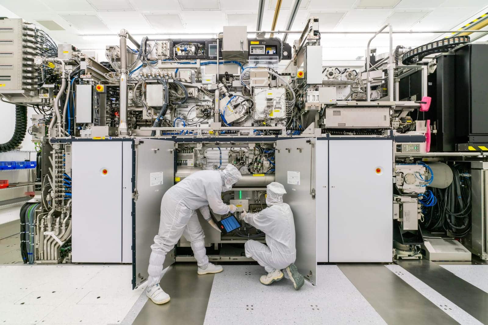
Machines that manufacture the world’s most advanced chips have become one of the most delicate pieces of the tech economy. They don’t train AI models, don’t appear in data centers, nor reach the end consumer, but without them, processors powering smartphones, GPUs, servers, connected cars, or AI accelerators wouldn’t exist. At the center of this chain is ASML, the Dutch company that dominates EUV lithography and has already mapped out its roadmap until the next decade.
The image presented by ASML at SPIE 2026 summarizes well where the industry stands: low numerical aperture EUV tools will continue evolving for years, High-NA systems are entering early production, and Hyper-NA ideas are emerging as a possibility beyond 2030. The transition won’t be smooth or quick. It’s most likely to see a prolonged coexistence between DUV, Low-NA EUV, and High-NA EUV, with each technology reserved for layers where it offers the best cost, performance, and complexity trade-offs.
DUV remains the quiet backbone of manufacturing
Media attention tends to focus on EUV, but immersion DUV lithography remains essential for volume chip production. Even at advanced nodes, many chip layers don’t require the most expensive machines or the finest exposures. They are printed with DUV systems—more mature, plentiful, and with well-understood manufacturing economics.
ASML closed 2025 with €32.7 billion in revenue, a gross margin of 52.8%, and a net profit of €9.6 billion. That year, it recognized revenue from 48 EUV systems and 279 DUV systems, a significant portion of which were immersion tools. The company also ended the year with a order backlog of €38.8 billion, reflecting both AI chip demand and pressure from manufacturers to expand capacity in advanced nodes and memory.
Immersion DUV hasn’t disappeared because it remains useful and profitable. In mature nodes, it supports much of the production for automotive, industrial, consumer electronics, and sensors. In advanced nodes, it can be combined with EUV for less demanding layers or even stretched via multipatterning—though this technique adds steps, masks, cycle time, and defect risk. That’s where EUV makes more sense: it not only allows smaller patterns but also simplifies processes that, with DUV, would be too lengthy or costly.
China has been a major buyer of DUV in recent years, partly due to the inability to access EUV and the tightening export controls. Since September 2024, the Netherlands has required licenses to export certain models like the TWINSCAN NXT:1970i and 1980i systems to specific destinations—a restriction added to existing controls over more advanced DUV models and EUV. This has reinforced DUV tools’ strategic value: they are not the most advanced frontier but remain a path to producing competitive chips when more process steps and lower efficiencies are acceptable.
Low-NA EUV still has significant potential
Current EUV lithography, with low numerical aperture or Low-NA, operates with an NA of 0.33 and uses 13.5 nm wavelength light. It was the technology that helped solidify the 5 nm, 3 nm nodes, and part of the transition to 2 nm. According to its own annual report, ASML is the sole global manufacturer of EUV systems, giving it enormous influence over the schedules of TSMC, Intel, Samsung, SK hynix, and other industry players.
ASML’s roadmap shows that Low-NA won’t retire soon. The NXE:3600D is associated with 3 nm generation and 1B memory, while the NXE:3800E increases productivity to over 220 wafers per hour and transitions toward 2 nm and 1C memories. The first-quarter 2026 results presentation indicates that ASML has already released an upgrade package for the NXE:3800E, boosting its throughput from 220 to 230 wafers per hour with similar overlay performance.
Next would come the NXE:3800F, planned for 2027-2028, followed by the NXE:4200G around 2029-2031, and the NXE:4200H in the 2031-2033 window. These systems aim for better overlay performance and increased productivity, with the NXE:4200H targeting at least 330 wafers per hour. Later, a high-productivity platform, the NXE:4600, targets 400 wafers per hour or more.
This extension is logical: Low-NA remains a highly valuable tool when combined with software, metrology, and computational lithography. Optical correction techniques, mask optimization, and process control allow existing systems to be pushed further without wholesale infrastructure changes. TSMC exemplifies this with its A16 and A14 strategies: they do not plan to use High-NA EUV at these nodes and prefer to adopt the new generation when clear technical and economic benefits are evident.
This stance doesn’t mean TSMC will abandon High-NA forever. For the world’s largest contract manufacturer, the equation isn’t yet clear. If multipatterned Low-NA EUV can produce satisfactory results despite more steps, then High-NA must justify its price, size, and the modifications needed in manufacturing facilities.
| Technology | Numerical aperture | Intended role | Main advantage | Main limitation |
|---|---|---|---|---|
| Immersion DUV | 1.35 | Mature layers and many non-critical layers | Cost and maturity | Complex multipatterning at fine nodes |
| Low-NA EUV | 0.33 | Current and upcoming advanced nodes | Good productivity and installed base | Requires multipatterning for the most demanding patterns |
| High-NA EUV | 0.55 | Critical layers below 2 nm and advanced DRAM | More resolution in a single exposure | Cost, size, and manufacturing integration |
| Hyper-NA | >0.7, under study | Potential technology for the 2030s | Higher optical resolution | Physical challenges, resists, pellicles, and cost |
High-NA enters the scene but doesn’t replace everything
High-NA EUV is ASML’s significant optical leap. Moving from 0.33 to 0.55 NA enhances resolution to about 8 nm and enables printing features with a single exposure that might otherwise require double patterning with Low-NA. ASML introduces the EXE:5200B system, designed for 2 nm logic nodes and advanced DRAM. The company claims it offers 40% higher image contrast than NXE systems, allowing features 1.7 times smaller and a transistor density 2.9 times higher in a single exposure.
This system is no minor upgrade; High-NA systems are large, expensive, and challenging to install. Intel has been the most aggressive adopter, using the EXE:5200B as a development tool for Intel 14A. Acceptance was completed at the end of 2025, with production risk scheduled for 2027. For Intel, High-NA isn’t just lithography; it’s a means to regain technological credibility vis-à-vis TSMC.
Samsung and SK hynix are also beginning to move. SK hynix installed a High-NA system at its M16 plant in Icheon for future-generation DRAM, while Samsung is evaluating High-NA for its most advanced nodes. In memory, the technology is especially attractive as AI-driven demand for high-bandwidth memory (HBM), high-performance DRAM, and finer processes accelerates.
ASML’s roadmap includes the EXE:5200C, EXE:5200D, and EXE:5400E, with progressive productivity improvements. Additionally, a high-productivity platform, the EXE:5600, aims for 250 wafers per hour or more. The message is clear: High-NA isn’t a standalone experiment but a family of tools that ASML intends to bring to high-volume manufacturing.
Deployment will be selective. High-NA will likely focus on the most demanding layers, where it reduces steps and complexity. The rest will be handled with Low-NA EUV or DUV. Although this approach may seem less elegant than full substitution, it aligns better with economic realities: each layer should be manufactured with the most cost-effective tool, not necessarily the newest.
Hyper-NA and alternatives: promise vs. physics
Beyond High-NA, ASML and partners are exploring Hyper-NA concepts with apertures over 0.7. In theory, these would allow further reductions in feature sizes. In practice, they introduce increasingly challenging physical problems: shallower depth of focus, thinner photoresist films, stochastic defects, stricter mask and pellicle requirements, and even more complex optics.
The discussion surrounding Hyper-NA highlights a tough truth: each new lithography generation offers improvements but at rising costs. It’s not enough to develop a more extreme lens. The EUV source must deliver sufficient power, masks must withstand the exposure, pellicles must transmit light without degrading, resist materials must work with ultrathin films, and all of this must deliver good wafers at a justifiable cost.
Alternatives exist, though none seem poised to displace ASML in advanced logic. Canon’s nanoimprint lithography system, FPA-1200NZ2C, uses mechanical pattern transfer instead of optical projection. It shipped a unit to the Texas Instruments Electronics Institute in 2024 and claims potential for reducing consumption and cost. Generally, its best fit appears to be repetitive pattern applications, like memory or certain manufacturing steps, rather than high-volume logic where defects and overlay are critical issues.
The bottom line for the market is that ASML will remain hard to replace. Its business isn’t just about selling new machines; its installed base—including service and upgrades—reached €8.2 billion in 2025 and grows as factories leverage existing equipment more intensely. In early 2026, ASML raised its revenue forecast to €36-40 billion, with a gross margin of 51–53%, supported by AI demand and customer capacity expansion plans.
The practical takeaway: chip manufacturing doesn’t advance through clean jumps but layer by layer. DUV will continue operating. Low-NA EUV will keep expanding. High-NA will be adopted where justified by cost and benefit. Hyper-NA must prove it can overcome its physical limits. Meanwhile, each new AI, GPU, CPU, and memory generation will depend on an increasingly expensive, precise, and complex chain of machines.
Frequently Asked Questions
What’s the difference between DUV and EUV?
DUV uses deep ultraviolet light and is still used to produce many layers of current chips. EUV uses a much shorter wavelength, 13.5 nm, enabling smaller patterns with fewer steps on the most complex layers.
What is High-NA EUV?
It’s a next-generation EUV lithography system with a NA of 0.55. It improves resolution over current 0.33 NA systems and is designed for critical layers below 2 nm and advanced memory.
Why doesn’t TSMC want to use High-NA in A16 and A14?
TSMC believes it can continue progressing with Low-NA EUV, multipatterning, and computational lithography until High-NA offers clear advantages in cost, performance, and production. They plan to adopt it once measurable benefits are achieved.
Can Canon compete with ASML using nanoimprint?
Canon’s nanoimprint lithography offers an interesting alternative, but currently it seems more suited for specific applications rather than replacing EUV in high-volume advanced logic. Challenges include defects, alignment accuracy, and productivity.
via: ASML and tomshardware