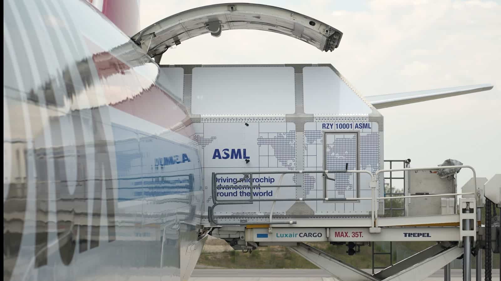
At the core of every digital device — from smartphones to supercomputers training artificial intelligence — lies an invisible protagonist: the microchip. The manufacturing of these components relies on a discipline called lithography, which involves etching tiny patterns onto silicon wafers. In this field, ASML, headquartered in the Netherlands, has established itself as the key player in the global industry. Its extreme ultraviolet lithography (EUV) technology is now indispensable, and its shift towards High-NA (0.55 numerical aperture) promises to define the future of semiconductors.
This article revisits the history of lithography, the pioneering role of ASML, and how the company has transitioned from working with mercury lamps to developing systems capable of projecting light with a wavelength of just 13.5 nanometers, more than 14 times shorter than deep ultraviolet (DUV) light.
From blue light to ultraviolet: origins
When ASML was founded in 1984, lithography used mercury vapor lamps. This technology produced blue light with a wavelength of 436 nm (g-line), sufficient for printing transistors of 1 micrometer (1,000 nm).
The industry soon demanded further miniaturization, leading to the shift to i-line (365 nm). These systems allowed reducing dimensions to 220 nm, a crucial step toward the modern digital era.
The pivotal advancement came in the 1980s with the use of excimer lasers, a more precise and stable light source. The first were KrF (krypton fluoride) lasers with 248 nm, which brought the industry down to 150 nm and later to 80 nm. The next generation, ArF (argon fluoride) lasers, reduced the wavelength to 193 nm, achieving feature sizes of 38 nm.
Each transition required investments in optics, light sources, and photosensitive materials, but all addressed the same need: making chips smaller and more powerful.
The arrival of EUV: a risky bet
The idea of using extreme ultraviolet light (EUV) began to be explored in the 1980s. The key was to utilize wavelengths of 13.5 nm, opening the door to printing features 14 times smaller than with DUV.

In 1994, a consortium of companies — led by ASML — achieved the first prototype demonstrating the viability of the concept. However, the journey was long and costly.
- In 2006, ASML shipped its first EUV demonstration tool to the College of Nanoscale Science & Engineering in Albany, NY, and to imec in Belgium.
- In 2008, despite the financial crisis, the first test chips with EUV were produced.
- In 2010, the TWINSCAN NXE:3100 system was delivered, marking a turning point in pre-production.
- In 2013, the NXE:3300 arrived, the first EUV system for production.
After years of doubts, delays, and adjustments, EUV lithography was solidified in 2016. In early 2020, ASML celebrated the shipment of its 100th EUV system.
How EUV light is created
The generation of EUV was no trivial challenge. No natural EUV sources exist on Earth, so ASML had to invent a radical technique:
- Melted tin droplets of 25 micrometers are fired at 70 meters per second.
- A primary laser pulse flattens each droplet into a disk shape.
- A second, much more powerful laser vaporizes the droplet, creating a plasma.
- This plasma emits 13.5 nm light, which is collected and directed toward the optical system.
This process repeats 50,000 times per second, making each machine a sort of “miniature star reactor” inside a clean room.
The leap to High-NA: the new frontier
With EUV technology mature, ASML moved toward a more ambitious version: EUV High-NA, increasing the numerical aperture from 0.33 to 0.55. This results in higher resolution, better contrast, and the ability to print 8 nm transistors with a single exposure.
The new EXE platform introduces:
- Redesigned optics in collaboration with ZEISS SMT, reducing aberrations.
- Faster wafer and reticle stages, increasing productivity.
- Almost three times higher density capacity compared to conventional EUV systems.
The first High-NA system was delivered in December 2023, and mass production is expected to begin in 2025–2026.
Impact on the semiconductor industry
The adoption of EUV, especially High-NA, is redefining the roadmap for manufacturers like Intel, TSMC, and Samsung.
- Intel has confirmed that its 14A node will utilize High-NA, albeit at a higher cost, raising questions about profitability.
- TSMC remains cautious, possibly delaying adoption and continuing to optimize conventional EUV to keep prices competitive.
- ASML becomes a geostrategic actor: no other supplier manufactures EUV, giving Europe a unique position in a sector dominated by Asia and the U.S.
However, the cost is monumental. Each High-NA scanner costs around $380 million, compared to the $235 million for conventional EUV. Despite this, manufacturers understand that without this technology, it would be impossible to continue shrinking transistors and keep Moore’s Law alive.
ASML: 40 years of innovation
Since its founding in 1984, ASML has evolved from building systems with mercury lamps to becoming the sole provider capable of delivering EUV at scale globally. Today, its machines are present in all cutting-edge chip factories and serve as a technological bottleneck: without them, there would be no smartphones, servers, or artificial intelligence as we know it.
The future lies in pushing the boundaries of physics and economics: more precise lithography, higher productivity, and sustainable costs. The challenge is immense, but ASML has already demonstrated that, in this field, it can achieve the impossible.
FAQs about ASML and EUV lithography
What does EUV lithography mean?
EUV (Extreme Ultraviolet Lithography) is a chip manufacturing technique that uses 13.5 nm ultraviolet light to print transistors much smaller than those made with previous methods.
What’s the difference between conventional EUV and High-NA EUV?
High-NA increases the numerical aperture from 0.33 to 0.55, allowing higher resolution and transistor densities nearly three times greater.
Why are ASML’s EUV machines so expensive?
Because they combine atomically precise optics, extreme vacuum systems, high-power lasers, and plasma sources that replicate complex physical processes. Each unit costs between $235 million and $380 million.
When will High-NA enter mass production?
The first systems have already been delivered, and mass production is expected between 2025 and 2026, playing a key role for nodes like Intel 14A.