China may have taken — at least in the lab — a step that for years seemed out of reach: a working prototype of extreme ultraviolet (EUV) lithography. The information, published on December 16, 2025 by DigiTimes Asia and attributed to an R&D environment in Shenzhen, is light on technical details and does not mean a machine ready to mass-produce chips, but it marks a psychological turning point: a message that the “core” of EUV could be entering the realm of possibility.
In the industry, however, the question is not whether a prototype exists, but whether it can become an industrial system capable of large-scale production with performance, stability, repeatability, and cost compatible with a modern factory. And that’s where the real challenge begins.
Why EUV redefines the landscape of AI chips
EUV is the method that has enabled continued progress toward leading-edge nodes (and with it, improved density, efficiency, and performance). In practical terms, this translates to more computing power per watt, a critical variable in AI: training and deploying models has become a battle over energy, costs, and silicon availability.
If China manages to close the EUV gap, the potential impact would be twofold:
- Industrial: unlocking faster iterations at advanced nodes within its technological frontier.
- Geopolitical: reducing the effectiveness of export control bottlenecks, which today revolve around technologies like EUV.
But even in the optimistic scenario, this isn’t an immediate “game over.” A prototype can demonstrate a physical principle; a production-worthy machine must prove years of reliable operation.
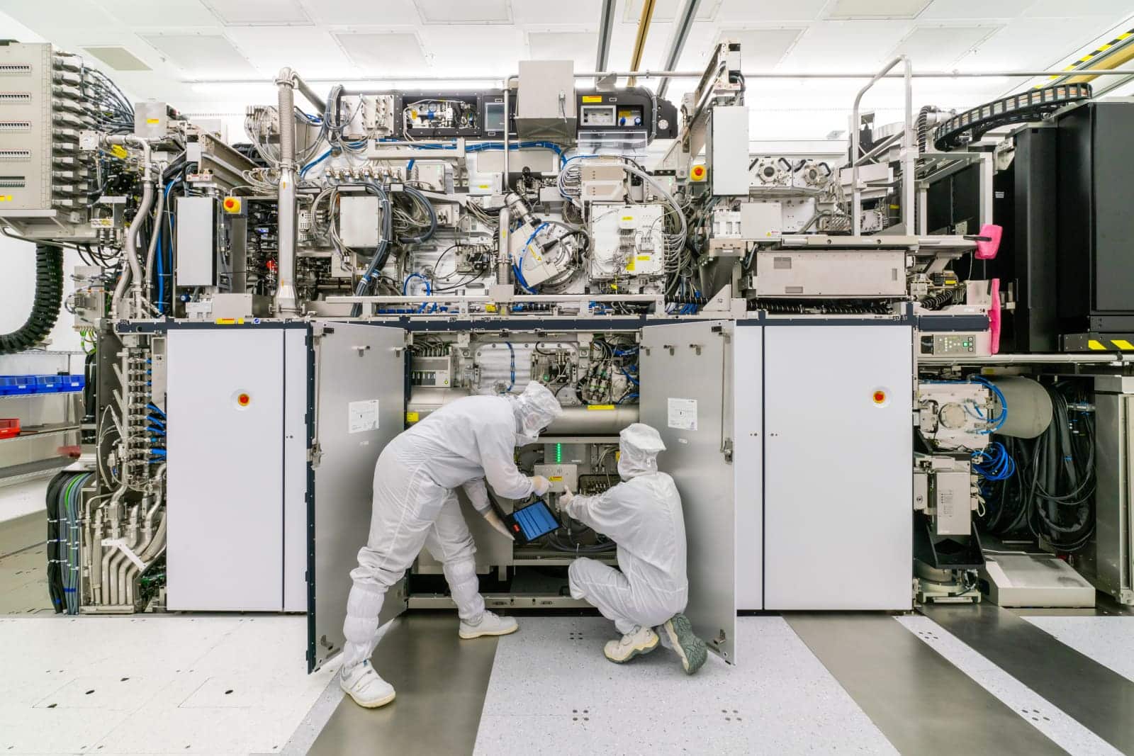
Prototype is not production: the real bottlenecks
Turning EUV into a “factory-ready” tool is among the most complex engineering tasks on the planet. It’s not just “deep ultraviolet light.” It’s an ecosystem of nearly impossible components:
- Stable EUV light source (with industrial power and availability).
- Reflection optics of extremely high precision (EUV doesn’t work like classical optics: it doesn’t “pass through” lenses, it bounces off special mirrors).
- Contamination control and mirror degradation management.
- Resists, masks, and metrology at the highest standards, plus a supply chain capable of maintaining extreme tolerances.
That’s why the industry tends to view these announcements as directional signals, not conclusive victories. A prototype might be real and still years away from a tool that can sustain the pace of a major foundry.
China’s “Plan B” was already underway: pushing DUV and multiplying steps
Even without EUV, China has been exploring alternative routes to manufacture advanced chips: more processes, more steps, and greater complexity to compensate for the lack of EUV with deep ultraviolet (DUV) lithography and multi-patterning techniques.
A recent example was presented by SiCarrier, a Shenzhen-based equipment firm, claiming it can help manufacture advanced semiconductors using domestic tools and alternative processes to EUV — with the usual trade-offs: increased complexity and potentially lower yields.
This strategy aligns with an uncomfortable reality: even without EUV, you can get close, but you pay in time, costs, variability, and overall capacity. In AI, where every month matters, that penalty is significant… but sometimes preferable to complete dependence on a blockade.
So, why does this prototype force us to “rethink the order” of AI chips?
Because it shifts the conversation. Until now, the dominant narrative was: “without EUV there’s no future at the leading nodes.” The emergence of a prototype (if confirmed and advanced) suggests a new framework:
- Short-term: still dominated by the status quo — industrial EUV, installed capacity, and operational know-how.
- Medium-term: becomes more uncertain — if China improves DUV + multi-patterning and begins to mature EUV, it could gain strategic leverage.
- Long-term: pathways diverge — leadership won’t just be about “who has the best GPU,” but “who controls the entire manufacturing ecosystem,” including equipment, materials, metrology, and software.
In essence: the “order” of AI development isn’t solely defined by chip design, but by who can sustainably produce chips when market pressures and political constraints intensify.
Frequently Asked Questions
What does it mean that China has a “EUV prototype”?
It means a functional lab system capable of demonstrating the principles of EUV lithography, but it doesn’t imply an industrial machine ready to produce high-performance, reliable chips on a large scale.
Could China produce cutting-edge chips without EUV?
They can approach it using DUV and multi-patterning, but usually at the cost of more manufacturing steps, increased complexity, and potentially lower yields. Chinese companies have publicly defended alternative routes along those lines.
Does this already affect the AI GPU market?
Not immediately. The current market dynamics are driven by actual production capacity and supply chains. If the prototype proves viable, its strategic implications are more about expectations than immediate availability.
What’s the biggest challenge to “industrialize” EUV?
The combination of: stable light sources, ultra-precise optics, contamination control, materials (resists and masks), metrology — all integrated to operate continuously with minimal tolerances. In EUV, scaling up is often harder than invention itself.
If you like, I can adapt it further to a more aggressive “tech-opinion” style or a more neutral “industry/business” tone, with additional emphasis on how this impacts data centers, cost per token, and technological sovereignty.