
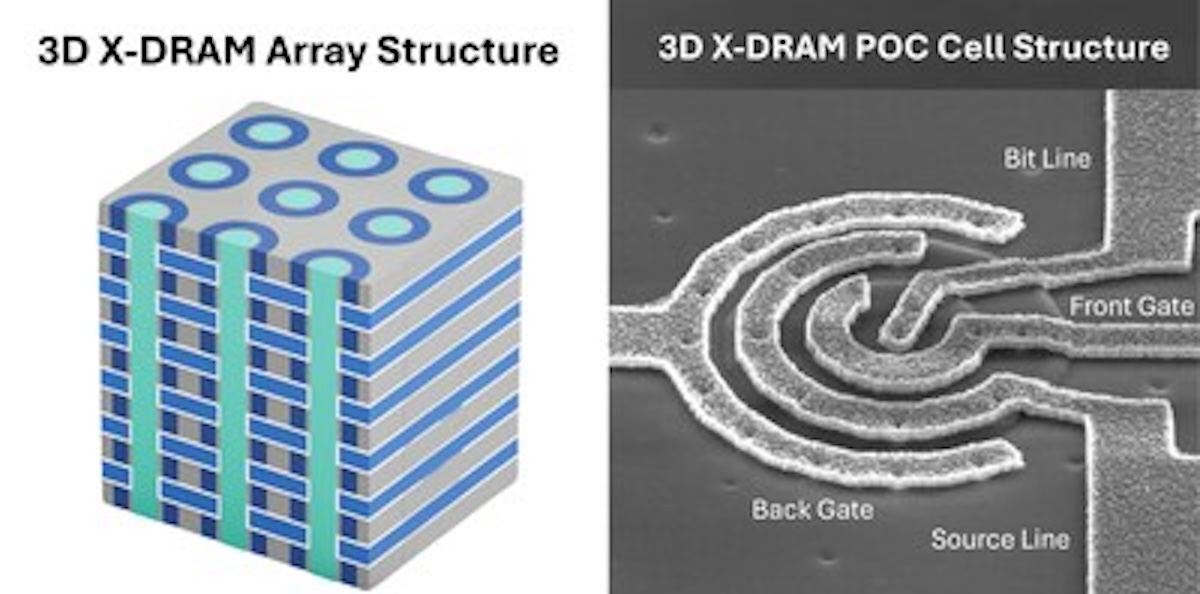
AMD has put numbers to the potential of one of the technologies that could change memory in future AI accelerators. The company estimates that a 3D DRAM architecture connected through hybrid bonding could be up to 17 times more energy-efficient than an HBM stack built on microbumps. The idea is appealing for systems where moving data is consuming more and more energy, though major thermal, manufacturing, and reliability hurdles still stand in the way of any near-term replacement for HBM.
3D DRAM in 20 seconds
- AMD estimates up to 17x better energy efficiency versus microbump-based HBM.
- The approach physically moves DRAM closer to the processor through much denser copper connections.
- Hybrid bonding shortens the distance and the energy needed to move each bit.
- Temperature, manufacturing yield, and contamination remain major obstacles.
- HBM will keep playing an essential role in upcoming generations of AI accelerators.
The figure also needs to be read with some caution. AMD hasn’t announced a commercial 3D DRAM product with that advantage, or a date for bringing one to market. It’s an estimate of what a hybrid-bonded architecture could achieve, not a claim that a commercial memory already consumes 17 times less than HBM.
AMD’s own current strategy shows that HBM is still far from obsolete. The CDNA 5 architecture integrates 432 GB of HBM4 spread across 12 stacks and reaches 23.3 TB/s of bandwidth. AMD also announced a partnership with Samsung in March to supply HBM4 for its Instinct MI455X accelerators.
The real question lies further ahead: what happens when continuing to increase HBM’s capacity, bandwidth, and stack count starts running into physical and energy limits.
From placing memory next to the processor to stacking it on top or underneath
HBM already uses a three-dimensional architecture. Several layers of DRAM are stacked vertically and communicate through silicon vias, known as TSVs (Through-Silicon Vias). The stacks are then placed next to the processor inside an advanced package.
The advantage over conventional DDR is considerable. AMD, for example, credits its Versal HBM parts with HBM2e for up to six times more bandwidth and 65% lower energy consumption per bit than certain Versal Premium configurations using external memory.
3D DRAM takes that proximity considerably further.
Instead of keeping memory stacked next to the processor and communicating with it through the package, the idea is to integrate logic and memory vertically, drastically cutting the physical distance data has to travel.
That’s where hybrid bonding comes in.
Current generations of HBM mainly rely on small physical connections known as microbumps. They work, but they impose limits on the minimum distance between connections, interconnect density, and energy efficiency. That’s precisely why Samsung and SK hynix have been cautious about rushing hybrid bonding into HBM itself.
Hybrid bonding removes those small solder points and establishes direct copper-to-copper connections between the surfaces of the chips.
The potential result is a much higher connection density. With thousands or millions of extremely short links, each one can operate at a relatively moderate speed and still deliver enormous aggregate bandwidth.
That also cuts the energy needed to move each bit.
And that variable is becoming just as important as raw compute capacity.
AI accelerators can perform enormous numbers of operations per second, but they need to continuously feed their compute units with weights, activations, and other data. If moving that information between memory and processor consumes too much electricity, improving the compute units alone stops solving the problem.
d-Matrix’s example shows where memory could be headed
The idea has already started leaving the lab.
d-Matrix recently unveiled Raptor, an AI inference accelerator that combines a compute chip built on a 4nm process with DRAM designed specifically for the system.
Both components are joined vertically.
The company has measured roughly 0.37 picojoules per bit on its vertical interface, compared with around 2.4 pJ/bit used as a reference figure for moving data to HBM4’s base die.
According to figures presented by d-Matrix, the system reaches 100 TB/s of bandwidth with 32 GB of memory per card. Those are vendor-supplied numbers for a different architecture than AMD’s theoretical proposal, so they shouldn’t be confused with the 17x improvement figure. They do, however, show why vertical integration is generating so much interest.
Samsung is exploring a similar path. At Hot Chips 2026, it presented a strategy in which future generations could pack increasingly more logic into the memory subsystem and, eventually, place DRAM directly on top of the processor.
The company also acknowledges the problem that immediately shows up when you do that: heat.
Heat is precisely this architecture’s biggest enemy
Putting memory on top of a processor looks simple in a diagram, but an AI accelerator can dissipate hundreds of watts.
DRAM is sensitive to temperature. Its cells store information using small electrical charges that need periodic refreshing. As temperature rises, charge retention can degrade, increasing refresh requirements.
There’s also a second thermal problem during manufacturing itself.
Hybrid bonding requires extremely flat, clean surfaces. After the initial contact between materials, thermal processes are used to achieve a reliable bond between the copper connections.
Those temperatures can affect DRAM’s characteristics.
Solving the problem means finding bonding processes that work within thermal budgets compatible with memory while still producing reliable connections over the device’s entire lifespan.
It also has to be solved how heat is subsequently extracted from the stack.
One possibility is to flip the architecture. Instead of placing memory on top of the logic that generates the most heat, designs can be built where DRAM sits below the processor, or where the thermal path finds a more direct route to the cooling system.
There’s no universal solution, since power density, layer count, materials, cooling, and package design all come into play.
A microscopic speck of dust can turn a chip into scrap
The other challenge is less visible, but can matter just as much economically.
Hybrid bonding demands extraordinarily high flatness and cleanliness.
Surfaces must align with enormous precision so the copper connections meet correctly. Contamination of just a few nanometers can prevent certain areas from bonding properly.
That problem takes on a different scale once millions of components are being manufactured.
A technology can work perfectly in the lab and still be economically unviable if the defect rate is too high. The more layers added and the more complex the connections, the more manufacturing yield matters.
The industry has spent years developing hybrid bonding for various applications, and commercial uses already exist, but applying it to complex logic-plus-multilayer-DRAM structures introduces new challenges around yield, cost, inspection, reliability, and heat dissipation.
That’s why it’s premature to present 3D DRAM as an immediate replacement for HBM.
HBM still has a long road ahead
The search for alternatives doesn’t mean HBM has reached the end of the line, either.
HBM4 is just starting to roll out in next-generation accelerators, and manufacturers are already working on later generations. Hybrid bonding itself could eventually end up being used within future HBM generations too.
AMD is specifically betting on HBM4 for CDNA 5, while Samsung, SK hynix, and other manufacturers are researching increasingly integrated structures.
The most likely scenario isn’t a sudden replacement, but a gradual evolution.
HBM can keep increasing capacity and bandwidth while specialized architectures with DRAM directly integrated into the logic emerge alongside it. Other paths also exist, from near-compute memory to CXL (Compute Express Link) for expanding or sharing large pools of memory.
The underlying reason is the same one every time: in AI systems, it’s no longer enough to build processors that can compute faster.
You also have to move gigantic amounts of information between memory and compute units, and do it while consuming a reasonable amount of energy.
A 3D DRAM capable of coming close to the improvement AMD has floated would change that equation. But it will first have to prove it can be manufactured at scale, run for years under high thermal loads, and offer enough capacity at a competitive cost.
Until then, that 17x figure represents the potential of an architecture, not the specs of a memory you can buy today.
Frequently asked questions
What is 3D DRAM memory?
It’s an architecture that aims to integrate layers of DRAM vertically, extremely close to the processing logic. The goal is to reduce the distance data has to travel and greatly increase the connection density between memory and processor.
Is it really 17 times more efficient than HBM?
AMD has pointed to a potential of up to 17 times compared with a microbump-based HBM architecture. It shouldn’t be read as a comparison between two equivalent commercial products, or as an improvement already available in accelerators.
Will HBM disappear once 3D DRAM arrives?
Not in the short term. HBM4 is part of the next generations of AI accelerators and keeps evolving. 3D DRAM represents one possible direction for future architectures.
What’s currently stopping DRAM from being built directly on top of processors?
The main obstacles include temperature, DRAM’s sensitivity during the manufacturing process, the precision hybrid bonding requires, manufacturing yield, and extracting heat when memory and logic are stacked together.
