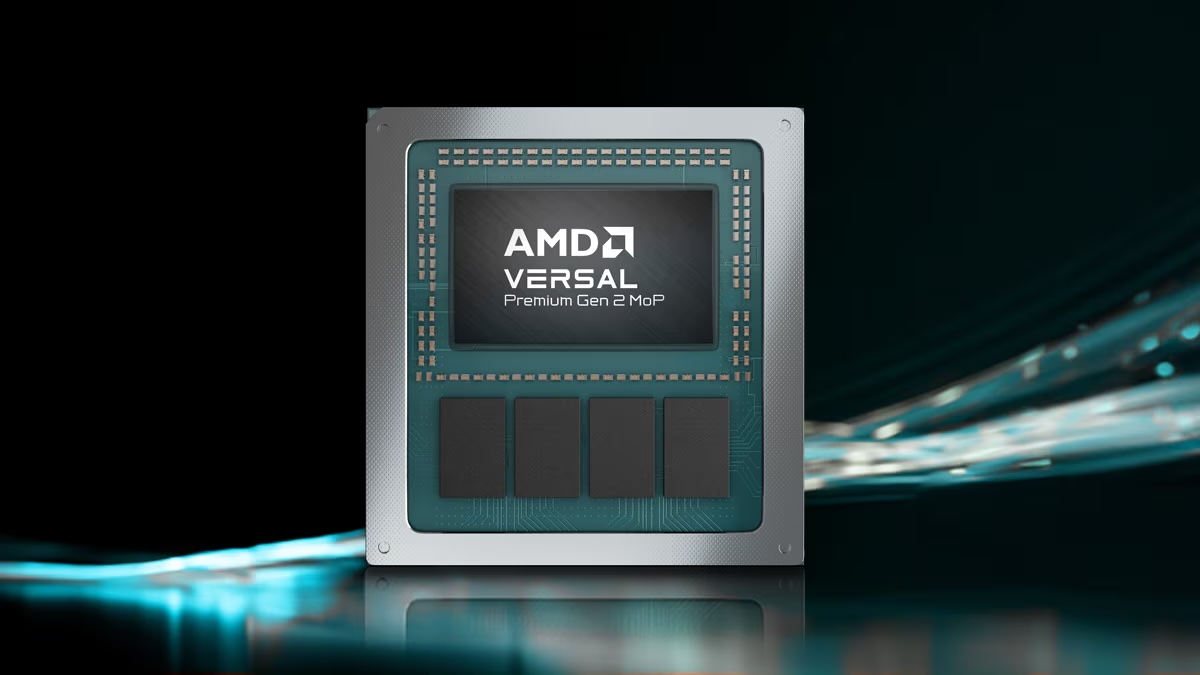
AMD has announced Versal Premium Gen 2 Memory on Package (MoP), a new variant of its adaptive SoCs that integrates LPDDR5X memory directly within the package. The technical idea is straightforward to explain but has significant implications for systems where every millimeter of board space, every watt, and each nanosecond matter: bringing memory closer to the chip to move data with higher bandwidth, simpler design, and less surface area used.
The company claims that this architecture allows for the integration of up to 32 GB of LPDDR5X within a single package, offering up to 288 GB/s of bandwidth and reducing PCB area by as much as 60% compared to designs with external memory, based on AMD’s internal measurements. The new devices target markets where fast, compact memory is as critical as computational capability: physical AI, networking, test and measurement, professional video, secure communications, and aerospace and defense systems.
The announcement does not directly compete with large datacenter accelerators using HBM. AMD proposes a different approach for long lifecycle products, industrial environments, and embedded designs that cannot be redesigned every few years at the pace of high-bandwidth memory used in large-scale AI.
Less board space, more bandwidth, and reduced design risk
In many advanced embedded systems, the bottleneck isn’t just computing power but also how data is fed into the chip. Placing high-speed memory outside the package requires designing complex PCB routes, signal validation, electrical behavior simulation, integrity checks, and accepting re-spin risks if something doesn’t work as expected.
AMD’s MoP approach reduces this burden by bringing LPDDR5X directly into the SoC package. By removing some high-speed memory routing from the PCB, manufacturers can shorten design cycles and lessen PCB-level validation. AMD presents this as a way to accelerate market entry and lower risks in products where redesigns are costly and could delay certifications or deployment.
| Feature | AMD Versal Premium Gen 2 MoP |
|---|---|
| Integrated memory | Up to 32 GB LPDDR5X |
| Bandwidth | Up to 288 GB/s |
| Area savings | Up to 60% less PCB space, according to AMD |
| LPDDR5X speed | Up to 9,000 Mb/s |
| Connectivity | PCIe 6.0 and CXL 3.1 up to 64 Gb/s in hard IP |
| Operating temperature | -40°C to 110°C |
| Lifecycle support | Over 15 years |
| Sampling | End of 2026 |
| Production | Second half of 2027 |
This approach opens the door to form factors where discrete memory complicates design, such as EDSFF or 3U VPX, common in dense and demanding environments. For telecommunications, defense, or industrial systems, reducing area without sacrificing bandwidth may be more valuable than maximum capacity.
An alternative for products that cannot rely on HBM cycles
HBM memory dominates much of the discourse around AI accelerators, especially in training and inference of large models. However, its roadmap is heavily centered on data centers and rapid refresh cycles. This doesn’t fit well with sectors designing products to operate for 10, 15, or more years.
AMD emphasizes this point. Versal Premium Gen 2 MoP uses LPDDR5X and offers long-cycle support, exceeding 15 years, to reduce the risk that memory availability forces redesigns prematurely. In industrial equipment, defense, aerospace, or critical communications, supply stability can be as important as technical specs.
The operating temperature range, from -40°C to 110°C, also places these devices outside the controlled environment of a data center rack. We are talking about systems that can operate in the field, in vehicles, remote stations, communication platforms, or systems that must stay on in harsh conditions.
Connectivity is another key point. Versal Premium Gen 2 MoP integrates PCIe 6.0 and CXL 3.1 up to 64 Gb/s in hard IP, making it easier to transfer data at high speeds and connect with AMD EPYC CPUs or with expansion and memory pooling modules via CXL. AMD already positioned the Versal Premium Series Gen 2 as a family oriented toward data-intensive applications, supporting PCIe Gen6, CXL 3.1, LPDDR5X, and DDR5.
Built-in security for communications and sensitive workloads
The announcement also features several platform-level security functions. AMD mentions PCIe Integrity and Data Encryption (IDE), introduced with PCIe 6.0, to help protect in-transit data at the link layer from physical attacks. It also includes DDR memory encryption through integrated controllers and high-speed cryptographic engines 400G designed for secure processing without sacrificing performance.
These features align with the target markets. In secure communications, defense, aerospace, or critical infrastructure, moving data quickly isn’t enough. It must be protected during transit, attack surfaces minimized, and performance maintained under encryption. In these environments, security isn’t an afterthought but a system requirement.
The combination of high bandwidth, compact size, and security controls can be particularly useful in physical AI workloads where models and sensors work close to the real world: industrial vision, signal analysis, communications, professional video, autonomous systems, or edge acceleration. Not all of these workloads need a GPU cluster; many require real-time data processing within a compact form factor and controlled power consumption.
Development with Vivado and Vitis, no need to start from scratch
AMD aims to ease adoption by maintaining continuity with its tools. Customers can begin development with standard Versal Premium Series Gen 2 devices, which are already shipping, and leverage existing workflows in Vivado and Vitis, compatible IP, and reference designs. The goal is that those already working with the Versal family won’t need to relearn everything to adopt the new MoP variants once available.
The roadmap sets the timeline: Versal Premium Gen 2 MoP devices will start sampling in late 2026, with production shipments planned for the second half of 2027. This timeline positions the technology within the design horizon of systems currently defining architecture, validation, and long-term availability.
This kind of announcement reflects a broader trend in semiconductors: not all innovation is about larger chips or more HBM memory. There’s also innovation in packaging, integration, area reduction, connectivity, and design simplification. For certain markets, bringing memory closer to compute and reducing engineering load on the PCB can be as impactful as increasing TOPS or TFLOPs.
AMD is positioning Versal as an intermediate space between FPGAs, adaptive SoCs, data acceleration, and long-cycle embedded platforms. With MoP, it aims to give designers a more compact and stable way to build high-bandwidth systems without the complexity of external memory or reliance on data center memory cycles.
Frequently Asked Questions
What is AMD Versal Premium Gen 2 MoP?
It is a variant of the Versal Premium Gen 2 adaptive SoCs that integrates LPDDR5X memory within the package to boost bandwidth and simplify design.
How much memory does it include?
AMD indicates up to 32 GB of LPDDR5X, with bandwidth up to 288 GB/s.
Why not use HBM?
AMD favors their integrated LPDDR5X approach here to provide lower design risk, support for over 15 years, and better fit for industrial, defense, and long-cycle embedded products.
What are the benefits compared to external memory on the PCB?
Reduces area, eliminates some high-speed routing, simplifies validation, and can shorten development cycles.
When will it be available?
AMD plans to start sampling by late 2026, with production shipments in the second half of 2027.
via: AMD