The pressure from Artificial Intelligence is starting to be felt in materials that rarely make headlines. This time, it’s not about GPUs, HBM memory, or lithography equipment, but about copper-clad laminates known as CCLs and special glass fibers used in substrates that support advanced chips. According to industry sources cited by The Elec, delivery times for some semiconductor CCLs have lengthened from about two weeks to six weeks.
The situation doesn’t yet amount to a production shutdown. substrate manufacturers are maintaining safety stock levels and several suppliers are expanding capacity. However, this shift is significant because it illustrates how the demand for AI servers is shifting supply chain stress toward basic materials that are hard to substitute and require lengthy qualification processes.
What is CCL and why has it become so important?
CCL, or Copper Clad Laminate, is a board made from an insulating material coated with copper layers. It serves as the base for printed circuit boards and substrates that host various semiconductor devices. In simple terms, it’s one of the physical layers that enable electrical signals to travel reliably within increasingly dense electronic systems.
Its manufacturing combines prepreg—a fiberglass fabric impregnated with resin—and copper sheets bonded through heat and pressure. The final product must withstand demanding thermal processes, maintain mechanical stability, and support increasingly finer circuits. In everyday applications, these requirements are already crucial. For high-performance AI chips, servers, and high-speed networks, they become much more stringent.
This is where T-Glass comes into play—a low thermal expansion fiberglass. Its role is to reduce substrate deformation when exposed to high temperatures. This stability facilitates the production of finer circuits and larger surface-area substrates—becoming increasingly necessary in advanced encapsulations, server modules, and large chips.
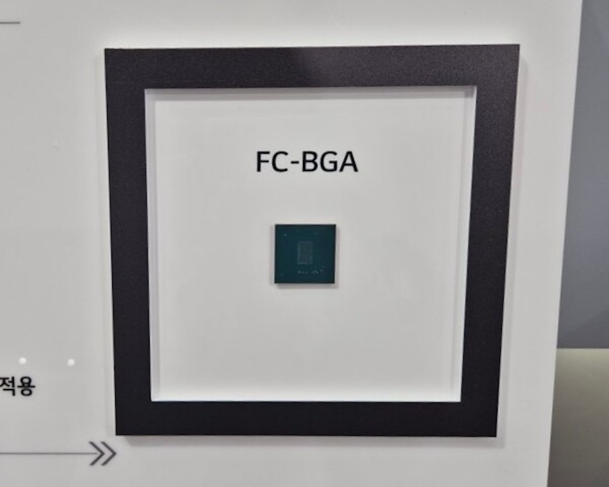
Until recently, T-Glass was used more selectively in premium substrates. Now, its use is expanding across more categories driven by increasing integration, the need for better heat management, and the growing size of AI chips. Materials once reserved for high-end substrates like FC-BGA and FC-CSP are now appearing in server modules and memory substrates as well.
The challenge is that supply cannot suddenly increase. In the most advanced market segments, Japanese company Nittobo holds a very strong position in T-Glass and has obtained quality certifications from major industry clients. Nitto Boseki describes T-Glass as a highly elastic material with low thermal expansion, essential for high-density encapsulation substrates. This technical specialization complicates quick substitution by alternative suppliers.
Premium demand also shifts common materials
The pressure isn’t limited to the most advanced products. Growing orders for premium CCLs are also affecting more common materials based on E-Glass, a standard fiberglass used in mid- and low-range products. If manufacturers concentrate lines, capital, and shifts on higher-margin laminates, the available capacity for basic products diminishes.
This dynamic has been observed during previous periods of semiconductor supply chain tension. When a premium technology consumes industrial capacity, secondary effects reach seemingly more commonplace components. In this case, CCLs for AI, servers, and high-speed networks are competing for materials, equipment, and processes with less profitable segments.
Provider interest confirms this market trend. For example, Doosan recently announced a 180 billion won investment in a CCL plant in Thailand focused on AI infrastructure and networking equipment, according to South Korean media. Lotte Energy Materials and Doosan Electronics BG also signed an agreement to develop low-loss HVLP copper sheets and CCLs, materials relevant for high-speed data transmission.
The copper foil itself is also a key detail. In plates and substrates for AI servers, signal integrity is fundamental. Surface roughness, dielectric losses, thermal stability, and the ability to maintain performance at high frequencies all directly impact the functionality of networking systems, accelerators, memory modules, and multilayer boards.
For this reason, the market is looking beyond total manufacturing capacity. It’s not enough to produce more generic CCLs; manufacturers need to produce CCLs with very specific properties, validated by demanding clients and suitable for high-density designs. Certification can take months, and some large clients prefer to avoid risks with untested materials on critical platforms.
A bottleneck that shouldn’t be overstated, but also shouldn’t be ignored
The most cautious interpretation is that the sector is experiencing a period of strain, not a collapse. Sources cited by The Elec indicate that substrate manufacturers still have reasonable inventories and that material suppliers are expanding capacity. This reduces the immediate risk of production interruptions.
Still, moving from delivery times of two weeks to six weeks impacts planning. substrate manufacturers need to purchase earlier, secure contracts, adjust inventories, and prioritize customers. For chip and server designers, the message is clear: the supply of encapsulation and PCB materials is now part of the industrial risk associated with AI.
This phenomenon aligns with a broader trend. For months, discussions have focused on shortages of HBM memory, CoWoS capacity, accelerator availability, and data center construction. Now, attention is also shifting to less visible layers: special glass, copper sheets, resins, lamination equipment, organic substrates, and validation processes.
Suppliers are responding. Nittobo announced in 2025 an expansion of production for special glass fabrics, with an investment of 15 billion yen, to meet the growth in encapsulation substrates for advanced semiconductors. Other manufacturers in Taiwan and China are also working on alternatives, though entering critical supply chains requires consistent quality, industrial capacity, and approval from end customers.
The increase in CCL delivery times shows that AI infrastructure is built on a supply chain broader than usually imagined. An AI server doesn’t rely solely on its main chip; it needs boards, substrates, connections, thermal materials, and components capable of supporting speeds, temperatures, and densities that only a few years ago were reserved for niche applications.
If demand continues growing at this pace, advanced PCB and substrate materials could become another focal point for manufacturers, hyperscalers, and infrastructure providers. It may not be the most visible bottleneck, but one that could significantly influence deployment timelines once all other components are secured.
Frequently Asked Questions
What is a CCL in semiconductors?
A CCL is a copper-coated laminate used as the base material to manufacture printed circuit boards and substrates where various electronic components and semiconductors are integrated.
Why is AI increasing the demand for CCL?
AI chips and servers require larger, more stable, and denser substrates with materials capable of withstanding high temperatures, supporting fast signals, and enabling very fine circuits.
What is T-Glass?
T-Glass is a low thermal expansion fiberglass that helps reduce deformation in substrates exposed to heat, improving stability in advanced encapsulation.
Is there a severe shortage of CCL?
Currently, the situation is better described as supply tension. Lead times have extended, but manufacturers maintain safety stocks and suppliers are expanding capacity.
via: thelec