
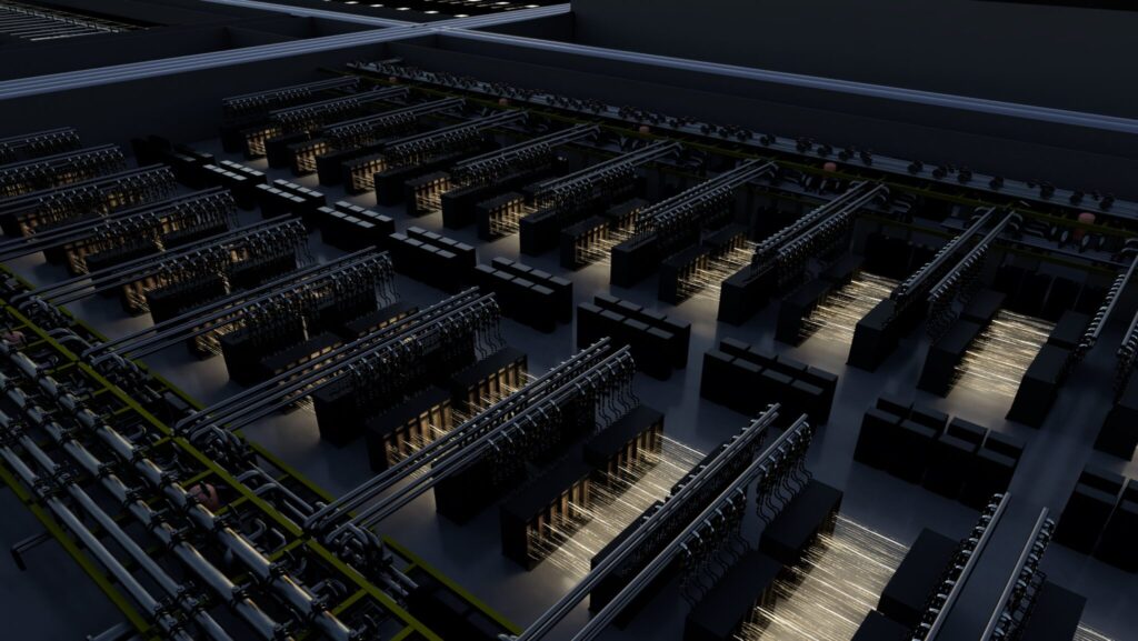
NVIDIA is expanding the reach of NVLink Fusion, their proposal for integrating custom accelerators or XPUs into AI infrastructures built around their technology. The company proposes that hyperscalers and in-house chip developers can retain their processors while adopting NVIDIA-made elements for interconnection, CPUs, rack systems, cooling, power, and managing large AI data centers.
The key points of NVIDIA NVLink Fusion in 20 seconds
- NVLink Fusion enables the integration of custom XPUs within NVIDIA’s NVLink infrastructure.
- The sixth generation of NVLink supports domains of 72 accelerators, with future configurations up to 1,152.
- NVIDIA assures that XPU-to-XPU latency is three times lower than conventional Ethernet alternatives.
- Manufacturers can reuse MGX architecture, cooling, power, networking, and suppliers.
- Partners mentioned by NVIDIA include Intel, MediaTek, GUC, Quanta, and Annapurna Labs.
This move is especially relevant given current market trends. Major cloud providers are increasingly investing in developing their own accelerators to reduce costs, tailor hardware for specific workloads, and decrease dependency on general-purpose GPUs.
Google has been developing its TPUs for years, AWS offers Trainium and Inferentia, and Microsoft has Maia. Meta is also working on its MTIA family. Simultaneously, semiconductor companies like Broadcom and Marvell see growing opportunities in designing custom ASICs for large infrastructure operators.
NVIDIA appears to anticipate continued growth in this market. Their response with NVLink Fusion aims to enable a third-party designed accelerator to still depend significantly on NVIDIA’s infrastructure.
NVLink opens up to accelerators that are not NVIDIA GPUs
This approach addresses a well-known challenge in large AI systems: building a good accelerator is only part of the necessary process to deploy it at scale.
A hyperscaler must also solve communication between accelerators, CPU integration, horizontal scaling networks, rack design, power distribution, liquid cooling, storage, security, management software, and a supply chain capable of producing thousands of systems.
NVLink Fusion aims to provide some of that infrastructure as a platform to incorporate custom processors.
The core remains NVLink, NVIDIA’s high-speed interconnect used so multiple accelerators can operate as a larger computational domain.
According to company data, the sixth-generation NVLink offers high-speed, low-latency communication within a domain of 72 XPUs. NVIDIA claims that transfers between XPUs can have end-to-end latency three times lower and packet rates ten times higher than conventional Ethernet-based solutions.
These figures are provided by NVIDIA and should be understood within the context of the configurations compared by the manufacturer, not as a universal advantage over all Ethernet architectures.
The company also envisions significant future evolution. Their roadmap includes NVLink configurations supporting up to 1,152 accelerators and incorporating integrated optics.
Scalability is especially important for models like Mixture of Experts (MoE), systems with trillions of parameters, and agent-based applications. When accelerators need to exchange large amounts of data constantly, interconnect performance can become a limiting factor on silicon utilization.
NVIDIA also aims to enter data centers with its own XPUs
NVLink Fusion has an enterprise-oriented view that goes beyond purely technical specs.
For years, NVIDIA’s AI growth has been directly related to selling their GPUs. The expansion into custom chips presents a different scenario: a hyperscaler might choose to use an ASIC designed for specific workloads instead of buying another NVIDIA accelerator.
NVLink Fusion enables NVIDIA to participate partially in that infrastructure even if the main processor was designed by another company.
The manufacturer offers various options. A custom XPU can connect to the NVLink domain and also use NVLink-C2C for communication with NVIDIA’s Vera CPUs or other compatible processors in the ecosystem.
NVIDIA estimates that NVLink-C2C can be up to six times more energy-efficient than PCIe interfaces for inter-processor communication, though this is based on NVIDIA’s own testing conditions.
The list of companies NVIDIA mentions regarding NVLink Fusion highlights how wide their expansion ambitions are.
Intel participates as a CPU architecture and technology provider. MediaTek and GUC are involved in developing custom ASICs. Quanta contributes to manufacturing and integration, and Annapurna Labs, owned by Amazon, publicly supports the approach.
The involvement of Amazon is notable because AWS is one of the leading developers of proprietary silicon for AI applications.
NVLink Fusion thus offers a sort of intermediate ground: using a proprietary accelerator without developing the entire surrounding infrastructure from scratch.
Rack becomes a shared platform
This strategy extends beyond NVLink itself. NVIDIA aims to standardize at the rack level and later, within the data center.
XPU-based systems can leverage the NVIDIA MGX architecture and the supply chain used for platforms like Vera Rubin NVL72, including racks, cooling solutions, power distribution, and future 800V DC power designs.
NVIDIA argues that such compatibility would allow building facilities before the final accelerator configurations are even decided.
This is key because data center timelines differ greatly from silicon development cycles. Securing power, designing cooling, or constructing a facility can take years, while accelerator generations evolve much faster.
With a common architecture, NVIDIA suggests that GPUs and XPUs share physical characteristics of the rack, cooling, power, networking, and management systems. Operators could subsequently adjust the mix based on workload demands or hardware availability.
Their approach also includes digital modeling of entire data centers via NVIDIA DSX and its Omniverse-based blueprints, enabling virtual testing of gigawatt-scale AI installations before physical deployment.
Reference racks will favor liquid cooling and modular trays for maintenance without halting the entire system.
Software complements this strategy: NCCL handles distributed workloads within NVIDIA environments, while Dynamo and NIXL are aimed at disaggregated architectures. Mission Control manages clusters, telemetry, and diagnostics.
This approach positions NVIDIA differently from traditional practices. If hyperscalers continue increasing their use of proprietary processors, NVIDIA can offer the full infrastructure connecting, powering, cooling, and managing those chips.
This also explains why NVLink Fusion might be a key element in the company’s evolving business model. NVIDIA no longer only competes to determine which accelerator performs calculations; it also aims to keep its architecture central around chips named by other companies.
Frequently Asked Questions
What is NVIDIA NVLink Fusion?
NVLink Fusion is a platform that enables integration of custom accelerators or XPUs into NVIDIA’s interconnection and infrastructure environment. Manufacturers can retain their own silicon while utilizing components like NVLink, compatible CPUs, MGX, and other rack design elements.
Does NVLink Fusion require the use of NVIDIA GPUs?
Not necessarily. One of its goals is to allow the integration of third-party developed XPUs within NVIDIA-based infrastructure.
How many accelerators can NVLink connect?
The sixth generation supports domains of 72 XPUs. NVIDIA’s roadmap includes future configurations supporting up to 1,152 accelerators and the use of integrated optics.
Why is NVLink Fusion significant for NVIDIA?
Because it enables NVIDIA to participate in data centers where large cloud providers increasingly use custom chips. Even if the accelerator isn’t an NVIDIA GPU, other parts of the infrastructure can still leverage NVIDIA’s technology.
via: blogs.nvidia
