
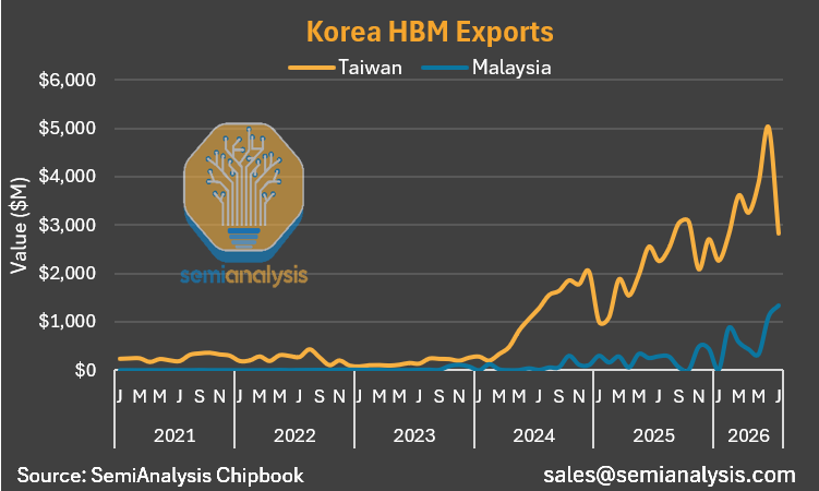
The sharp increase in South Korean exports of HBM memory to Malaysia is sending an unusual signal within the semiconductor supply chain. Data from SemiAnalysis Chipbook shows that these shipments are now about $1.3 billion, while those headed to Taiwan have dropped from over $5 billion to less than $3 billion in recent months. The growing hypothesis is that part of this memory is reaching Intel facilities to be integrated through advanced packaging technologies like EMIB and Foveros.
The key points about HBM movement to Malaysia in 20 seconds
- SemiAnalysis detects around $1.3 billion in South Korean chip exports to Malaysia.
- Shipments to Taiwan have decreased from over $5 billion to under $3 billion.
- Intel has a major advanced packaging infrastructure in Malaysia after investing $7 billion.
- AI is stressing TSMC’s CoWoS and creating opportunities for alternatives like EMIB and Foveros.
- Trade data points toward Intel, but does not identify the end recipient of each shipment.
The SemiAnalysis chart clearly illustrates this shift. Throughout 2024 and much of 2025, exports to Taiwan grew rapidly, while those to Malaysia remained significantly lower. In 2026, the two trends diverge: Taiwan continues to receive substantially higher value, but Malaysia shows a pronounced growth.
The significance lies in the product being moved. South Korea accounts for much of the global High Bandwidth Memory (HBM) production, an essential component for AI accelerators. Integrating multiple stacks of HBM around large computing chips requires advanced packaging technologies that have become a bottleneck in the industry.
Project Pelican Places Intel in the Right Position
Malaysia has been a key location for Intel’s industrial activity for decades, but the company is increasingly advancing operations there.
In 2021, Intel announced a $7 billion investment in Malaysia, including what it described as its largest advanced packaging facility for 3D technologies. The Penang complex covers over 65,000 square meters of cleanroom space across two manufacturing levels.
This expansion is known as Project Pelican and is prepared for operations involving technologies like EMIB and Foveros.
The coincidence between Intel’s increased capacity and the arrival of large volumes of HBM memory is hard to ignore.
TechPowerUp interprets SemiAnalysis data in that direction: TSMC does not have an equivalent advanced packaging facility in Malaysia, and other local players are still far smaller to handle such volumes.
However, customs data have a significant limitation. They show where the semiconductors are shipped, but do not alone reveal which company receives them or what final product incorporates them.
Therefore, attributing the $1.3 billion directly to Intel remains an inference.
What the SemiAnalysis data shows
| Indicator | Recent Situation | Why It Matters |
|---|---|---|
| HBM to Malaysia | ~$1.3B | Strong increase compared to previous years |
| Chips to Taiwan | <$3B | Had recently exceeded $5B |
| Intel’s investment in Malaysia | $7B | Includes large advanced packaging capacity |
| Intel technology | EMIB / Foveros | Designed for multi-chip systems and AI workloads |
| Final destination of HBM | Unconfirmed | Trade data do not specify clients |
Looking at the industrial context, it is increasingly likely that Intel is capturing new business opportunities.
In June, the company reorganized its Foundry division, placing advanced packaging under a dedicated leadership headed by Seok-Hee Lee. Intel justified this shift by emphasizing the growing importance of packaging for performance, energy efficiency, and heterogeneous integration in AI systems.
CoWoS Can No Longer Satisfy the Entire Demand
TSMC remains the market leader.
Its CoWoS (Chip-on-Wafer-on-Substrate) family is widely used to build some of the most sought-after AI accelerators. Different variants like CoWoS-S, CoWoS-L, and CoWoS-R enable integration of large compute chips with multiple HBM stacks within increasingly larger systems.
The paradox for TSMC is that its own technology is in such high demand that available capacity has become a constraint in recent years.
The AI arms race has shown that producing enough GPUs depends not only on advanced wafers but also on HBM, substrates, and the capacity to physically integrate these components.
This opens an opportunity for Intel that doesn’t necessarily involve taking clients away from TSMC.
If an accelerator designer can produce their dies but cannot find enough capacity to package them in time, having a second source becomes very attractive.
This is where EMIB (Embedded Multi-die Interconnect Bridge) comes into play.
Instead of using a large silicon interposer beneath different components, EMIB introduces small silicon bridges into the substrate at connection points requiring high density between dies.
Intel states that this technology has been in mass production since 2017 and can connect both logic-to-logic and logic-to-HBM. It also supports external silicon, which is especially important for Intel Foundry: a customer does not necessarily need to manufacture all their chips with Intel to use its packaging technology.
In addition, Intel offers Foveros for vertical integration and EMIB-T, an evolution incorporating Through-Silicon Vias (TSV) in the bridges.
Intel is explicitly targeting these technologies at the massive multi-chip systems needed for AI and high-performance computing. During their 2026 presentations, they showcased EMIB-T with packages up to 120 x 120 millimeters and capacity to integrate computing and memory surfaces exceeding nine reticles.
Intel’s Great Opportunity May Not Be Limited to Chip Manufacturing
This movement is particularly relevant for understanding Intel Foundry’s strategy.
When thinking about competing with TSMC, the focus is often on Intel’s 18A, 14A nodes, and which company boasts the best process node.
But packaging offers another entry point into the market.
An accelerator can contain dies produced by different foundries, memory from SK Hynix or Samsung, and various interconnection technologies. Someone has to turn these components into a functional system.
Intel aims to occupy precisely that role.
The company describes advanced packaging as a critical piece to overcome the physical limitations of manufacturing larger processors as a single silicon block. Foveros enables stacking chiplets, and EMIB connects them laterally with high bandwidth.
Moreover, Intel is expanding its ecosystem so other companies can design around these technologies. In July, Synopsys announced flows compatible with EMIB and EMIB-T, including multi-die systems linked to Intel’s 14A process.
Even Intel’s internal structure reflects this strategic focus. The company has separated advanced packaging into a dedicated activity with leadership specifically for it within Foundry.
HBM as a Map of the AI Industry
Tracking the movement of HBM provides an unusual way to see where accelerators are being built.
Memory produced in Korea is likely to travel to facilities where it will be integrated with computing chips. In recent years, a significant portion of this journey has led toward Taiwan, driven by TSMC and CoWoS.
Now, the growth of Malaysia introduces another relevant destination.
This does not yet prove that Intel is taking a market share from TSMC, nor does it clarify which clients are using Project Pelican, how many packages Intel is producing, or what its manufacturing yields are. These are fundamental data points for truly assessing the competitiveness of the operation, and they are not yet publicly available.
But it does suggest that the landscape for advanced packaging may be broadening.
And this is happening just as Intel is trying to turn one of its historical strengths—advanced packaging—into a third-party business. The company not only maintains EMIB and Foveros but continues developing EMIB-T, 3.5D integration, and new substrate technologies for ever-larger AI systems.
The big question will be whether the HBM increase to Malaysia is a temporary peak or the start of a sustained trend.
If it continues to grow alongside Intel’s increased production of Project Pelican, the US company might have found a particularly promising ground to regain relevance as a manufacturer: not necessarily replacing TSMC in transistors, but helping to solve the bottleneck that appears after fabrication.
Frequently Asked Questions
Why is HBM shipment to Malaysia increasing?
SemiAnalysis data shows a significant rise during 2026. The existence of new advanced packaging capacity from Intel makes Project Pelican one of the possible destinations, although trade data alone cannot confirm this directly.
What is Intel’s Project Pelican?
It is the expansion of Intel’s advanced packaging infrastructure in Malaysia, part of a $7 billion investment. It relates to advanced integration technologies like EMIB and Foveros.
Is Intel replacing TSMC and CoWoS?
There is not enough data to say for sure. TSMC remains dominant with high demand for CoWoS. What recent movements suggest is that Intel might be capturing part of the market’s growth or capacity TSMC cannot handle.
Why is packaging so important for AI chips?
Because modern accelerators combine multiple compute dies with several stacks of HBM. Technologies like CoWoS, EMIB, and Foveros enable these components to be interconnected with the bandwidth and efficiency needed to operate as a single system.
