
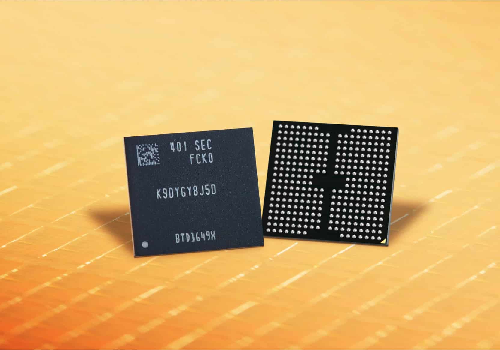
Samsung has leveraged Future of Memory and Storage (FMS) 2026 to showcase one of the industry’s most ambitious roadmaps in memory technology. The company revealed zHBM, a new high-bandwidth memory concept designed to be integrated directly onto AI accelerators, as well as introduced V10 BV-NAND, the industry’s first wafer-bonded NAND architecture with over 400 layers, and zNAND-O, a new proposal focused on edge AI workloads.
The key features of Samsung’s new memory in 30 seconds
- Samsung presents zHBM, an architecture that positions HBM memory directly on the AI accelerator.
- The company claims it could offer up to eight times the performance of HBM5 and increase density tenfold.
- They also announce V10 BV-NAND, the first NAND with over 400 layers based on wafer-bonding technology.
- The new generation boosts density by 58% compared to V9 and enhances read, write, and I/O performance.
- Samsung completes the roadmap with zNAND-O, aimed at real-time AI applications.
These innovations arrive at a time when the industry is seeking new ways to eliminate bottlenecks between processors and memory, one of the main challenges for training and deploying increasingly large AI models.
zHBM changes the traditional HBM memory architecture
Samsung’s main announcement was zHBM, a conceptual architecture that breaks away from the usual high-bandwidth memory design.
In current platforms, HBM chips are placed beside the processor or accelerator using advanced interposers. With zHBM, Samsung proposes stacking memory vertically directly on top of the AI accelerator, reducing the physical distance data must travel.
According to the company, this approach could significantly increase both bandwidth and energy efficiency for AI training and inference systems.
Samsung asserts that a future interface based on this architecture could achieve:
- Up to eight times the performance of HBM5.
- More than ten times the memory density compared to HBM5.
- An improvement of three times in energy efficiency.
- Over 50% lower thermal resistance, supporting the stability of high-capacity systems.
The company also suggests that the space between the accelerator and memory could be used to integrate custom IP blocks, tailoring each solution to different client needs.
However, it’s important to note that zHBM is currently a conceptual model, announced as part of Samsung’s technology roadmap, and not a commercial product with a launch date yet.
V10 BV-NAND surpasses 400 layers
The second major announcement is V10 BV-NAND, a new generation of flash memory that introduces for the first time a Bonding V-NAND (BV-NAND) architecture.
The main difference compared to previous generations is the use of a new wafer-bonding technology, where multiple wafers are physically joined to create NAND structures with significantly greater height.
Thanks to this design, Samsung exceeds 400 layers, marking a new industry milestone.
According to the company, V10 BV-NAND achieves:
- Approximately 58% higher density compared to V9.
- Improved read and write performance.
- Higher input/output (I/O) speeds.
- Reduced energy consumption.
These improvements are mainly aimed at future data center storage systems and AI applications.
zNAND-O targets edge AI applications
Samsung also showcased zNAND-O, another architecture still under development.
This is a V-NAND-based memory designed specifically for latency-critical applications like edge AI, where low response times are especially important.
Currently, Samsung is working on four- and eight-layer versions and believes it will offer better spatial efficiency, improved I/O performance, and lower response times compared to traditional NAND solutions.
A comprehensive strategy for AI data centers
Beyond these experimental developments, Samsung used FMS 2026 to update its commercial roadmap.
Solutions showcased include:
- HBM4E.
- HBM5.
- LPDDR5X-PIM, memory with integrated processing capabilities.
- Enterprise SSD units PM1763 and BM1773.
The company also emphasized its strategy as an integrated manufacturer, combining memory, chip fabrication, and advanced packaging technologies to deliver complete solutions for data centers and AI infrastructure.
The presentation confirms that the memory market is entering a new phase, where simply increasing layer count or chip speed is no longer enough. Manufacturers are now redesigning memory architecture itself to meet the growing demands for bandwidth, energy efficiency, and capacity dictated by AI accelerators.
Frequently Asked Questions
What is zHBM?
It is a new memory concept introduced by Samsung that proposes stacking HBM memory directly onto AI accelerators to reduce data travel distance and boost performance.
Is it commercially available?
No. Samsung has presented zHBM as a conceptual model within its future architecture vision for memory.
What does V10 BV-NAND offer?
It introduces a new wafer-bonding architecture surpassing 400 layers, and Samsung claims it increases density by 58% over the previous generation.
What is zNAND-O?
It is a developing NAND architecture designed for edge AI applications where low latency is especially critical.
