
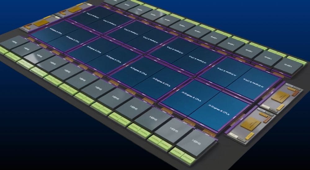
Intel Foundry has introduced a new architecture to manufacture chip packages up to 240 × 240 millimeters, roughly the size of a plate and equivalent to approximately 24 times the maximum exposure area of a conventional reticle. The company has not yet produced a full device of that size but claims to have solved one of the obstacles preventing progress toward it: encapsulating large sets of chiplets without leaving bubbles or gaps that could compromise reliability.
The key points of Intel’s giant chips in 20 seconds
- Intel designs packages up to 240 × 240 millimeters for AI and supercomputing.
- The architecture could incorporate dozens of chiplets, HBM memory, and I/O components.
- Gapless encapsulation has already been validated in designs exceeding seven reticles.
- Full packages would consume between 15 and 25 kW and require modular cooling.
- This is advanced research, not a commercial product ready for market.
The results come from two papers presented by Intel at the IEEE Electronic Components and Technology Conference (ECTC) in 2026. One describes the Hyper-Large Form Factor (HLFF) architecture, and the other focuses on the encapsulation process needed for such large sets to be manufactured reliably.
This advance does not eliminate all issues related to large-sized chips. Intel still needs to demonstrate the ability to produce the full package, power dozens of components, dissipate several kilowatts of heat, and keep a substrate flat, which could deform by several millimeters. What has been achieved addresses a specific, yet crucial, part of this pathway.
From monolithic chip to complete systems within a single package
The industry has been moving away from processors built on a single silicon piece for years.
Making larger monolithic chips decreases the number of units per wafer and increases the likelihood that any defect could render the entire component useless. It also forces the use of the same manufacturing process for blocks with different requirements.
Chiplets allow for dividing the design. Compute cores can be produced on an advanced node, while interfaces, cache, or certain controllers can use more economical processes. These pieces are then connected via advanced packaging technologies.
Intel already employs this approach with EMIB, a series of small silicon bridges embedded in the substrate, and Foveros, which allows vertical stacking of chips. The HLFF architecture takes this concept to a much larger scale.
The studied designs would integrate arrays of compute chiplets, high-bandwidth memory stacks (HBM), and I/O blocks on a single platform. EMIB-T bridges with metal layers under two micrometers would provide internal connection speeds exceeding 64 Gb/s per channel.
The goal is to reduce the distance between different blocks and prevent each accelerator from functioning as a completely separate unit. The closer the chiplets and memory are, the less energy is needed to move each bit, and the higher the overall bandwidth can be.
Intel is studying two configurations. The first uses EMIB-T bridges for all processor intercommunications, prioritizing performance and allowing redundant connections. The second routes some traffic through the substrate, with lesser physical complexity but some trade-offs in speed.
Encapsulation was one of the most challenging limits
After placing the chips on the substrate, the manufacturer must fill the small space beneath them with a material called underfill.
This compound protects solder joints, distributes mechanical stresses, and helps prevent damage during temperature changes. It is typically deposited around the chip edge and advances via capillarity through the available gap.
The process becomes more complex as the size of the set increases. Previous designs required the material to traverse about 22 millimeters. For current EMIB packages, Intel is working with distances exceeding 43 millimeters.
Longer journeys increase the risk that the compound does not reach all areas or leaves air pockets. These voids can become failure points as the chip heats up, cools down, or remains under load over years.
Intel has experimented with three variables: the material’s composition, the application method, and curing conditions.
They reduced the viscosity of the underfill to enable it to travel further, without removing enough particles to weaken its mechanical strength. Application shifted from solely edge dispensing to multiple points, including spaces between chips.
Finally, they adjusted temperature and curing time to ensure residual voids collapse after deposition. Initial tests showed defects with diameters up to 3.4 millimeters. After process modifications, Intel achieved void-free sets.
Intel has validated encapsulation over seven reticles
The work is not limited to simulations.
Intel has encapsulated a >5x reticle size EMIB package, consisting of 18 chips, including positions for 12 HBM stacks. The material traveled over 40 millimeters.
The company also achieved void-free results in an EMIB design formed by mosaics exceeding seven reticles. In Foveros 3D packages, they obtained clean encapsulations at scales of two and four reticles.
The Foveros two-reticle version also underwent reliability testing, including 700 thermal cycles and over 1,000 hours at high temperature, according to Intel. These results demonstrate the viability of the process at the tested sizes, but do not mean the 240 × 240 millimeter package is ready for production.
Intel clearly distinguishes these levels. Encapsulation has been validated up to sizes exceeding seven reticles, while the 24-reticle limit corresponds to the architecture’s HLFF boundary.
The company expects to surpass 12 reticles in the medium term and is exploring panel-scale formats that could approach 50 times a reticle’s area. These are developmental targets, not confirmed timelines for commercial products.
A 25 kW package requires redesigning power and cooling
Size is not the only challenge.
Intel estimates a full HLFF system could consume between 15 and 25 kW. A single unit would have power comparable to several current servers and create very different hot spots depending on the chiplet types in each zone.
A large, cold plate across the entire surface would not necessarily ensure uniform cooling. The proposal involves independent thermal modules, each with sensors and capacity to remove over 5 kW.
This approach would tailor cooling to each group of chips. A zone with compute accelerators could receive more airflow or operate at lower temperatures than a region dedicated to I/O.
Power delivery must also be closer to the silicon. Routing all current from the edges of a 240-millimeter package would cause losses and voltage drops. Intel proposes integrating silicon capacitors within the substrate and under the chips, with up to a millifarad of local storage per reticle-sized area.
Voltage regulators could be mounted on the package or integrated within. This would enable faster response to consumption changes when thousands of compute units start or stop loads.
Deformation is another concern. Materials in the substrate, chips, and encapsulant expand at different rates. Intel modeled a bend of up to seven millimeters at room temperature, enough to prevent electrical contact or separate the cooling system.
Solutions under consideration include thicker reinforcement rings, glass-core substrates, and solder balls of different sizes. During operation, the cooling system would exert a force exceeding 4,500 newtons to keep the entire set nearly flat.
Redundancy will be necessary to ensure manufacturability
With a package this large, the probability increases that some connections have defects.
Discarding the entire unit due to a faulty channel would make manufacturing prohibitively expensive. Therefore, Intel suggests adding spare communication paths alongside active ones.
Their calculations show that adding three to four extra channels per group of 64 would raise the performance from approximately 97% to over 99%.
A two-point difference might seem small, but it multiplies across hundreds or thousands of links. Redundancy allows disabling a defective connection and switching to another without losing the entire package.
This requires testing, detection, and reconfiguration mechanisms. It also increases surface area and complexity, so it must be balanced against the cost of manufacturing spares that may never be used.
Gigantic chips will also need co-packaged optics
Moving data within the encapsulation is only part of the challenge. Such a platform must communicate with other accelerators, storage systems, and external networks.
Intel believes that traditional electrical connections will face difficulties reaching the next target of 448 Gb/s per channel outside the package. Alternatives include co-packaged copper cables and co-packaged optics, known as CPO.
Optics would enable placing photonic interconnects near chiplets and reducing electrical trace lengths. Fiber would then carry traffic to other systems with lower losses and power consumption than long copper links.
This integration highlights that HLFF packages cannot be treated as standalone processors. Power distribution, cooling, memory, interconnection, and optics must be designed jointly.
Rio Rancho gains strategic importance within Intel Foundry’s plans
Intel is developing some of these technologies at their Rio Rancho facility in New Mexico, home to Fab 9, an advanced packaging plant.
The company has invested in expanding Foveros manufacturing and other integration technologies. Originally starting in the 1980s producing six-inch wafers, Rio Rancho now stands as one of Intel’s main US packaging sites.
The work presented at ECTC supports a part of Intel Foundry’s strategy beyond just transistor manufacturing. The company aims to offer process, advanced assembly, interconnects, and integration services for third-party-designed products.
Other manufacturers like TSMC, Samsung, ASE, and Amkor are also ramping up packaging capabilities. The rising demand for AI accelerators has made technologies like CoWoS, EMIB, and Foveros as significant as lithography nodes for production limits.
Intel has made a notable step by demonstrating void-free encapsulation in sets over seven reticles. The 24-reticle package has not yet been built nor publicly demonstrated under all required manufacturing conditions.
Nevertheless, this progress indicates the industry’s future direction: next-generation AI chips will resemble more a complete system assembled inside a package rather than a single piece of silicon. The limiting factor will shift from lithography exposure to how many chiplets can be interconnected, powered, and cooled as a unified system.
Frequently Asked Questions
Has Intel already manufactured a 240 × 240 millimeter chip?
No. Intel has proposed an architecture at that size and validated encapsulation processes in packages larger than seven reticles. The full 240 × 240 millimeter design is still in the research phase.
What does surpassing the reticle limit mean?
The reticle defines the maximum area a lithography machine can expose in a single shot. Advanced packaging allows combining several separately manufactured chips to create a system whose total surface exceeds that limit.
How much energy would these packages consume?
Intel estimates a full HLFF system could use between 15 and 25 kW, requiring integrated power supplies and modular liquid cooling.
What could be the uses for Intel’s giant chips?
The architecture is primarily aimed at AI accelerators, supercomputers, and high-performance computing systems needing large amounts of computation and HBM memory.
via: linkedin
