
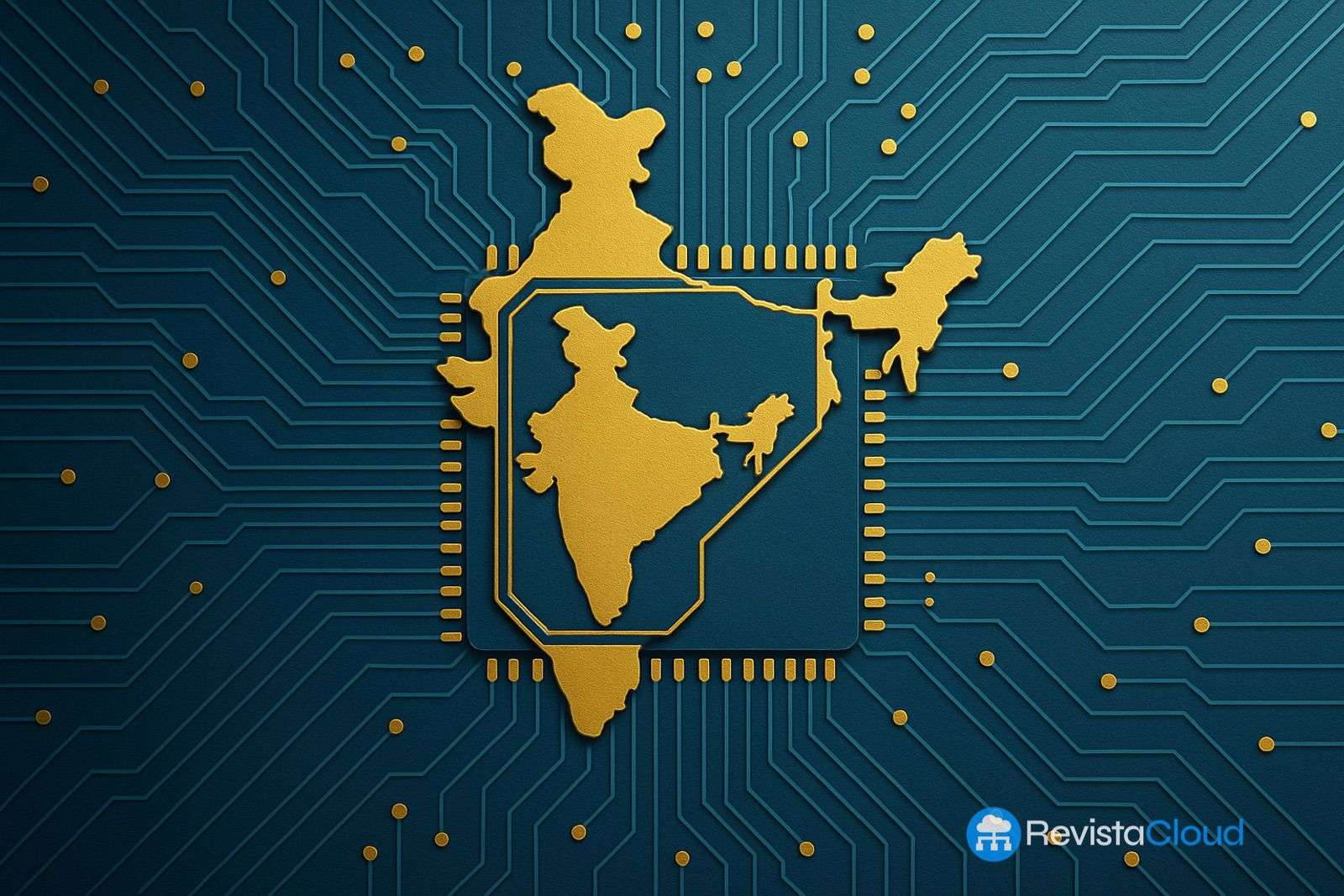
India wants to carve out a space in the global semiconductor supply chain, but it’s not starting with the most expensive and challenging part of the business. Its most immediate bet is something else: growth in OSAT and ATMP, that is, chip assembly, packaging, marking, and testing. It may seem like a less glamorous layer than manufacturing advanced wafers, but it’s a much more realistic entry point for a country aiming to build industrial capacity, talent, and credibility in semiconductors without waiting decades.
According to The Hindu BusinessLine, India has attracted around 64,000 crore rupees in announced investments in OSAT and ATMP facilities under the India Semiconductor Mission. Notable projects include Tata Electronics’ plant in Assam, CG Semi’s OSAT unit, Kaynes Semicon’s facilities, the HCL Group-Foxconn joint venture in Uttar Pradesh, and Suchi Semicon’s plant in Gujarat.
The logic is clear. A cutting-edge semiconductor fab can require between $10 billion and $25 billion or more, in addition to an extremely complex supply chain of equipment, materials, processes, and knowledge. An OSAT facility, on the other hand, can operate with significantly lower investments, shorter implementation timelines, and less technological risk. For India, it’s a way to start where the country can make progress first.
OSAT: less visible than a fab, but increasingly strategic
OSAT stands for Outsourced Semiconductor Assembly and Test. In practice, these plants receive pre-fabricated chips on wafers, dice them, encapsulate, connect, test, and prepare them for use in final products. ATMP, Assembly, Testing, Marking, and Packaging, follows a similar logic.
For years, this phase was seen as less strategic than wafer manufacturing. That perspective is changing. Advanced packaging has become essential for AI, automotive, industrial electronics, communications, sensors, and consumer devices. In many modern chips, performance depends not only on the fabrication node but also on how memory, logic, interconnects, and modules are integrated into the final package.
India seems to recognize that it doesn’t need to capture the entire supply chain from day one. It can start with a layer where demand already exists, where the country can connect its design talent with manufacturing capacity, and where reliance on imports remains high.
| Project | Approximate Investment | Location | Focus |
|---|---|---|---|
| Tata Electronics | 27,120 crore rupees | Assam | Assembly and packaging |
| CG Power / CG Semi | 7,584 crore rupees | Gujarat | ATMP/OSAT with Renesas and Stars Microelectronics |
| Kaynes Semicon | 3,307 crore rupees | Sanand, Gujarat | Wire bonding and substrate-based packages |
| HCL Group-Foxconn | 3,706 crore rupees | Uttar Pradesh | Display driver ICs and chip probing |
| Suchi Semicon | $100 million | Gujarat | High-volume OSAT for packages |
The Indian government has outlined several of these projects within its Semicon India program. Tata Electronics is developing a ₹27,120 crore facility in Assam with a capacity of 48 million units per day; CG Power is pushing forward a ₹7,584 crore unit in Gujarat with Renesas and Stars Microelectronics; Kaynes Technology is developing another plant in Gujarat for ₹3,307 crore, and the HCL-Foxconn joint venture in Uttar Pradesh has pledged ₹3,706 crore for display controller chips and related services.
India’s advantage: design, domestic demand, and diversification
India starts with an advantage that not all aspirants have: design talent. The local industry insists that the country already contributes more than 20% of the world’s semiconductor design talent. But designing chips alone isn’t enough if manufacturing, packaging, testing, and part of the supply chain are outsourced elsewhere.
This is where OSAT acts as a bridge. It connects design, validation, packaging, and testing. While it doesn’t instantly make India a complete semiconductor powerhouse, it provides a stronger position within a supply chain that companies are actively diversifying.
Domestic demand also plays a role. India is seeing growth in smartphones, consumer electronics, automotive, telecommunications, industrial equipment, defense, energy, and digital government projects. All these sectors consume chips. If the country can locally package and test some of these components, it can reduce reliance on imports and bring manufacturing closer to electronics producers.
The geopolitical context favors India. Many global companies are seeking alternatives to supply chains heavily concentrated in China, Taiwan, South Korea, or Southeast Asia. India may not replace that ecosystem overnight, but it can position itself as a credible secondary source in certain layers of the supply chain.
By 2025, Reuters reported approval of the HCL-Foxconn plant near Jewar Airport in Uttar Pradesh, with an investment of about ₹37,060 crore, aiming for a capacity of 20,000 wafers per month and 36 million display driver chips annually. Commercial production was expected by 2027.
The hard part: materials, equipment, and operational talent
The enthusiasm around OSAT shouldn’t obscure the challenges. Assembling and testing semiconductors demands precision, quality control, stable processes, specialized equipment, and a manufacturing culture very different from software. Having land, incentives, and demand alone isn’t enough.
A key obstacle will be the local supply chain. Many critical materials, equipment, substrates, chemicals, testing tools, and process components are still imported from global suppliers. If India wants to be more than just a subsidized assembly destination, it must develop local and regional suppliers around these plants.
Operational talent is another delicate point. The chip industry needs cleanroom technicians, quality control specialists, process engineers, maintenance personnel, reliability experts, packaging, electrical testing, and automation specialists. These profiles are built through technical training, industrial experience, and time.
The India Semiconductor Mission’s official goal is to build an ecosystem of semiconductor and display manufacturing in India, supported by incentive programs and project approvals. The mission’s webpage lists new approvals and agreements related to fabs, OSAT, ATMP, and materials—reflecting a broader strategy beyond just establishing a single plant.
OSAT can’t be the ultimate goal
Betting on OSAT makes sense as a first step, but not as the final aim. If India remains confined to assembly and testing, it will continue to depend on other countries for technologies, materials, equipment, IP, and wafer manufacturing.
The next leap must be in advanced packaging, substrates, specialized chemicals, precision equipment, EDA tools, design IP, advanced materials, power electronics, and selective wafer manufacturing—areas where the country can build a competitive advantage. Not everything needs to be at the most advanced node; there’s considerable value in power chips, automotive applications, sensors, analog, controllers, telecom, and industrial devices.
This nuance is important. The semiconductor race isn’t won only by manufacturing the smallest wafers in the world. It’s also about dominating high-volume, high-reliability components used in cars, factories, power grids, medical devices, consumer electronics, and industrial equipment.
India can carve out a reasonable space here. It’s not competing initially with TSMC at the most advanced nodes. Instead, it aims to become a reliable alternative for assembly, testing, packaging, and eventually specific parts of the supply chain where global demand continues to grow.
A more realistic industrial strategy than a spectacular one
The Indian case offers a lesson for any country discussing technological sovereignty. Not all semiconductor strategies start with a cutting-edge fab. Sometimes, the smartest approach is to begin with a less glamorous phase that’s more feasible to execute.
OSAT enables the creation of skilled jobs, attracting suppliers, training technicians, engaging with customers, learning manufacturing discipline, and building reputation. If the implementation succeeds, the country can progress in the supply chain. If it fails, at least the learning cost will be lower than trying to build a top-tier fab from scratch without an ecosystem.
India is making a pragmatic bet: start where it can produce sooner and use that as a foundation to scale. Success will depend on not settling for being a subsidized packaging shop, but turning these plants into the start of a complete industrial chain, with talent, indigenous technology, and local demand.
In semiconductors, arriving late doesn’t prevent competition, but it does require careful choice of entry point.
Frequently Asked Questions
What is an OSAT plant?
It’s a facility dedicated to the assembly, packaging, and testing of chips that have already been fabricated on wafers. It prepares semiconductors for use in final products.
Why does India prioritize OSAT over advanced fabs?
Because it requires less investment, carries lower execution risk, can start production sooner, and helps build critical capabilities in the supply chain.
How much investment has India attracted in OSAT and ATMP?
According to The Hindu BusinessLine, around ₹64,000 crore in announced projects under the India Semiconductor Mission.
Which companies stand out in this strategy?
Tata Electronics, CG Semi, Kaynes Semicon, HCL-Foxconn, and Suchi Semicon are among the most notable projects.
Is OSAT sufficient for semiconductor sovereignty?
No. It’s a useful first step, but India will also need capabilities in materials, equipment, design IP, advanced packaging, EDA, talent, and selective wafer manufacturing.
via: thehindubusinessline
